There are many kinds of electronic packaging substrates, and the commonly used substrates are mainly divided into plastic packaging substrates, metal packaging substrates and ceramic packaging substrates. Plastic packaging materials usually have low thermal conductivity and poor reliability, and are not suitable for high requirements. Metal packaging materials have high thermal conductivity, but the general thermal expansion coefficient does not match, and the price is high.
Ceramic substrates are commonly used in electronic packaging. Compared with plastic substrates and metal substrates, ceramic substrates have the following advantages :
(1) good insulation performance and high reliability;
(2) Low dielectric coefficient, high frequency performance;
(3) Low thermal expansion coefficient and high thermal conductivity;
(4) With good air tightness and stable chemical performance, it plays a strong protective role for the electronic system.
Therefore, it is suitable for aviation, aerospace and military engineering high reliability, high frequency, high temperature resistance, air tightness of the product packaging. Ultra-small chip electronic components are widely used in the fields of mobile communication, computer, household appliances and automobile electronics, etc., and their carrier materials are often encapsulated with ceramic substrates.
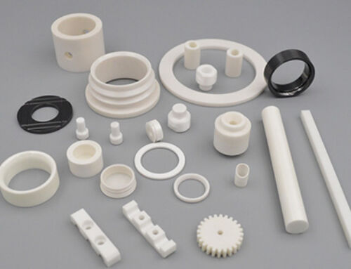
At present, several commonly used ceramic substrate materials for electronic packaging include alumina (Al2O3), aluminum nitride (AlN), silicon nitride (Si3N4), silicon carbide (SiC), boron nitride (BN), beryllium oxide (BeO).
Al2O3 ceramic substrate
Al2O3 ceramics generally refers to Al2O3 as main raw materials, mainly of alpha Al2O3 crystal phase, Al2O3 content in more than 75% of all kinds of ceramic, it has rich raw material sources, low cost, high mechanical strength and hardness, good insulation performance and good heat shock performance, chemical corrosion resistance, high dimensional accuracy, the advantages of good adhesion with metal, is a kind of comprehensive performance better ceramic substrate materials. Al2O3 ceramic substrate is widely used in electronic industry, accounting for 90% of the total amount of ceramic substrate, and has become an indispensable material for electronic industry.
Al2O3 ceramic substrates currently used are mostly multilayer substrates. Al2O3 content improves electrical insulation performance, thermal conductivity and impact resistance, but at the same time, it will lead to an increase in sintering temperature and production cost. In order to reduce the sintering temperature and ensure the mechanical and electrical properties of Al2O3 ceramic substrates, a certain amount of sintering AIDS, such as B2O3, MgO, CaO, SiO2, TiO2, Nb2O5, Cr2O3, CuO, Y2O3, La2O3 and Sm2O3, are often added to promote sintering.
Although Al2O3 ceramic substrate has large output and wide application, it is limited in the use of high frequency, high power and very large scale integrated circuit due to its higher thermal conductivity compared with silicon single crystal.
AlN ceramic substrate
AlN ceramic substrate is a new type of substrate material, the lattice constant of AlN crystals for a = 0.3110 nm, c = 0.4890 nm, hexagonal system, based on [AlN4] tetrahedron structure unit of wurtzite covalent bond compound, good thermal conductivity, a reliable electrical insulation, low dielectric constant and dielectric loss, non-toxic, and match the silicon thermal expansion coefficient and so on a series of excellent features, is considered to be a new generation of high integration semiconductor substrate and the ideal of the electronics packaging materials .
The preparation process of AlN powder, the core raw material of AlN ceramics, is complex, high energy consumption, long cycle and expensive. High cost limits the wide application of AlN ceramics, so AlN ceramic substrates are mainly used in high-end industries .
Si3N4 ceramic substrate
Si3N4 has three crystalline structures, namely phase, phase and phase, among which phase and phase are the most common forms of Si3N4, and they are all hexagonal structures. Si3N4 has many excellent properties, such as large hardness, high strength, small thermal expansion coefficient, small creep at high temperature, good oxidation resistance, good thermal corrosion performance and small friction coefficient. The theoretical thermal conductivity of monocrystalline silicon nitride is up to 400W/ (m·K), and has the potential to become a high thermal conductivity substrate. In addition, the thermal expansion coefficient of Si3N4 is about 3.0×10⁻⁶℃, which is well matched with Si, SiC, GaAs and other materials, making Si3N4 ceramics a very attractive substrate material for high strength and high thermal conductivity electronic devices [4].
However, Si3N4 ceramics have poor dielectric properties (the dielectric constant is 8.3, the dielectric loss is 0.001~0.1) and high production cost, which limits its application as an electronic encapsulated ceramic substrate.
SiC ceramic substrate
SiC ceramics have high thermal conductivity, which ranges from 100 w /(m·k) to 400W/(m·k) at high temperature, 13 times higher than Al2O3. Good anti-oxidation performance, decomposition temperature above 2500℃, in the oxidation atmosphere at 1600℃ can still be used; Moreover, the electrical insulation is good, and the thermal expansion coefficient is lower than Al2O3 and AlN. SiC ceramics have strong covalent bond characteristics and are difficult to be sintered. A small amount of boron or aluminum oxide is usually added as sintering AIDS to improve the density. Experiments show that beryllium, boron, aluminum and their compounds are the most effective additives, which can make the density of SiC ceramics reach more than 98% .
However, the dielectric constant of SiC is too high, 4 times that of AlN, and its compressive strength is low, so it is only suitable for low-density packaging but not high-density packaging. In addition to integrated circuit components, array components and laser diodes, etc., it is also used for structural parts with electrical conductivity.
BeO ceramic substrate
BeO is alkaline earth metal oxides in only six party wurtzite structure, because the BeO has wurtzite and strong covalent bond structure, and the relative molecular mass is low, therefore, have high thermal conductivity, BeO alumina is about 10 times, its thermal conductivity at room temperature can reach 250 w/(m K), and the thermal conductivity of the metal, and under the high temperature, high frequency, its electric performance, good heat resistance, heat resisting impact and delicate chemical stability.
Although BeO has some good properties, its fatal disadvantage is the extreme toxicity of its powder. Long-term inhalation of BeO dust will cause poisoning or even life-threatening, and will cause environmental pollution, which greatly affects the production and application of BeO ceramic substrate [5]. In addition, BeO is expensive to produce, which limits its production and application. Its use is limited to the following aspects: heat sinks of high-power transistors, heat sinks of high-frequency and high-power semiconductor devices, emission tubes, TWTS, laser tubes, klystron, etc. BeO ceramic substrates are sometimes used in avionics and satellite communications for high thermal conductivity and ideal high frequency characteristics.
BN ceramic substrate
BN can be crystallized in two different forms: hexagonal and cubic. Among them, the cubic crystal BN has high hardness and high temperature resistance of 1500~1600℃, which is suitable for superhard materials. Hexagonal BN can maintain high chemical and mechanical stability at very high temperature under correct heat treatment. The BN material has high thermal stability, chemical stability and electrical insulation, meanwhile, the thermal conductivity of BN ceramics is equal to that of stainless steel at room temperature, and the dielectric property is good. BN has better brittleness than most ceramics, smaller thermal expansion coefficient, strong thermal shock resistance, and can withstand sharp changes in temperature difference above 1500℃.
Both cubic BN and hexagonal BN are prepared under high temperature and high pressure, which are typical covalent bond crystals. Due to its high thermal conductivity, thermal conductivity almost does not change with temperature, small dielectric constant and good insulation performance, BN is applied to radar Windows, tube bases of high-power transistors, tube shells, heat sinks and microwave output Windows. But cubic BN is too expensive to be used in the production of high thermal conductivity ceramic materials. The mismatch between thermal expansion coefficient and silicon also limits its application .

-scaled-500x383.jpg)