전자제품용 실리콘 카바이드 세라믹 씰링: 전체 기술 가이드
전자 및 반도체 제조 산업은 부품 고장이나 미세한 오염으로 인해 전체 생산 배치가 망가져 수백만 달러의 비용이 발생할 수 있는 극도로 가혹한 조건에서 운영됩니다. 엔지니어들은 극심한 열 부하와 에칭 플라즈마의 공격적인 화학적 공격을 관리해야 하는 중대한 문제에 끊임없이 직면합니다. 그리고 웨이퍼 제조 환경에서의 고속 기계적 마모도 마찬가지입니다. 이러한 복합적인 문제에 대한 최적의 솔루션은 실리콘 카바이드 전자제품용 세라믹 씰링. 경도가 2500HV를 초과하고 열전도율이 150W/m-K에 육박하는 실리콘 카바이드(SiC)는 전자 등급 씰링과 관련된 거의 모든 지표에서 기존 금속 및 표준 세라믹보다 뛰어난 성능을 발휘합니다. 이 포괄적인 기술 가이드에서는 재료 특성, 비교 이점, 제조 워크플로우에 대해 자세히 설명합니다. 또한 첨단 전자 인프라에 SiC 씰링을 적용하는 데 필요한 정밀 가공 고려 사항도 설명합니다. R&D 또는 조달 팀에 허용 오차가 ±0.005mm에 불과한 초정밀 부품이 필요한 경우 고급 세라믹 전문가와 협력하는 것이 가동 중단 시간을 최소화하고 평균 고장 간격(MTBF)을 극대화하는 첫걸음입니다. 그레이트 세라믹에 문의 를 클릭하여 맞춤형 엔지니어링 요구 사항에 대한 견적서를 요청하세요.
머티리얼 속성
전자제품용 실리콘 카바이드 세라믹 씰 링의 적용은 전적으로 뛰어난 기계적, 열적. 그리고 전기적 특성 때문입니다. 반도체 패키징 및 웨이퍼 처리 장비에서 씰 링은 부식성이 강한 가스와 빠른 열 순환에 노출됩니다. 그리고 엄청난 마찰력에도 노출됩니다. 실리콘 카바이드는 다른 소재가 소성 변형이나 치명적인 열 충격을 받을 때에도 구조적 무결성과 치수 안정성을 유지합니다. 아래 표에는 소결에 대한 중요한 정량적 지표가 요약되어 있습니다. 실리콘 카바이드 전자 등급 씰링 애플리케이션에 활용됩니다.
| 속성 | 가치 | 단위 |
|---|---|---|
| 밀도 | 3.10 - 3.15 | g/cm³ |
| 경도 | 2500 - 2800 | HV |
| 굴곡 강도 | 400 - 450 | MPa |
| 골절 인성 | 4.0 - 4.5 | MPa-m½ |
| 열 전도성 | 120 - 150 | W/m-K |
| 전기 저항 | 10³ - 10⁶(조정 가능) | Ω-cm |
| 최대 작동 온도 | 1600 | °C |
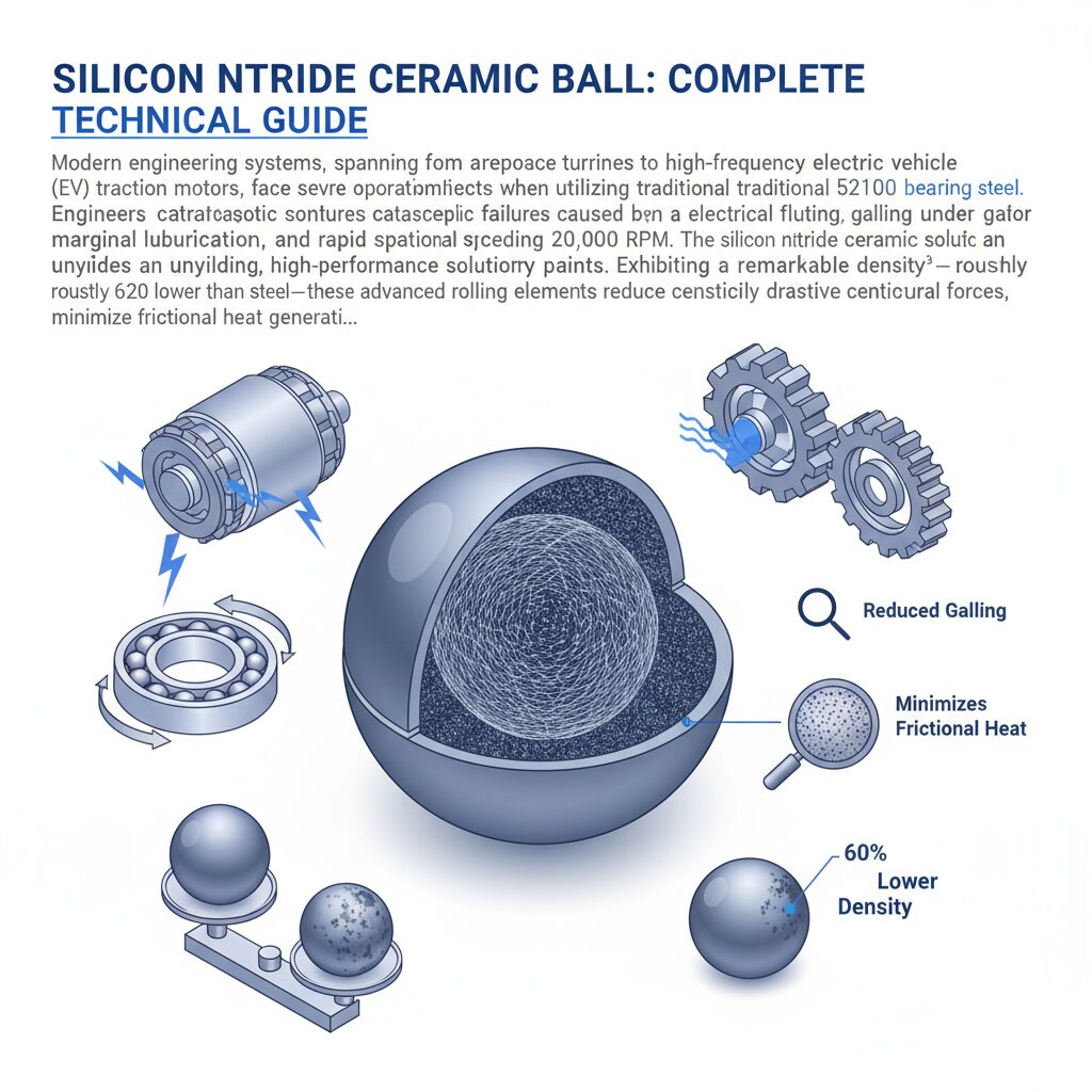
이러한 매개변수를 분석하면 이 소재가 이 분야를 지배하는 이유를 정확히 알 수 있습니다. 3.10g/cm³의 밀도는 부품의 경량화를 보장하여 최대 10,000RPM에서 작동하는 고속 로터리 씰 적용 분야에서 원심력을 줄여줍니다. 다이아몬드와 탄화붕소에 이어 두 번째로 높은 2500~2800 HV의 뛰어난 경도는 건식 작동 조건에서도 매우 낮은 마모율을 보장합니다. 전자제품용 실리콘 카바이드 세라믹 씰 링이 결합 표면에 대해 회전하면 마찰로 인해 국부적인 열이 발생합니다. 표준 산화물 세라믹보다 10배 가까이 높은 120-150W/m-K의 열 전도성 덕분에 이 열이 빠르게 방출되어 인접한 폴리머 오링이나 하우징 구성품의 열 저하를 방지합니다.
또한 도핑 및 소결 단계에서 전기 저항을 특별히 조정할 수 있습니다. 고순도 SiC는 반도체 역할을 하지만, 정전기가 쌓이면 10나노미터 트랜지스터가 포함된 웨이퍼가 즉시 파괴될 수 있는 마이크로전자 제조의 필수 요건인 정전기 방전(ESD) 안전 애플리케이션에 적합한 범위로 저항을 조정할 수 있습니다. 최대 연속 작동 온도가 1600°C에 달해 고온 화학 기상 증착(CVD) 공정 중에도 씰 링이 뒤틀리거나 가스를 배출하거나 기계적 강도를 잃지 않습니다.
다른 세라믹과의 비교
전자제품 제조를 위한 씰링 솔루션을 설계할 때 사양가들은 여러 가지 고급 세라믹을 평가하는 경우가 많습니다. 각 재료마다 고유한 틈새 시장이 있지만, 중요한 물리적 특성을 비교하면 거친 회전 및 정적 씰링 환경에서 실리콘 카바이드의 작동 우수성이 강조됩니다.
| 속성 | 실리콘 카바이드 | 알루미나 | 지르코니아 | 질화규소 |
|---|---|---|---|---|
| 열 전도성 | 120 - 150 W/m-K | 25 - 35 W/m-K | 2 - 3 W/m-K | 20 - 30W/m-K |
| 경도 | 2500 - 2800 HV | 1500 - 1650 HV | 1200 - 1300 HV | 1400 - 1600 HV |
| 골절 인성 | 4.0 - 4.5 MPa-m½ | 3.5 - 4.0 MPa-m½ | 8.0 - 10.0 MPa-m½ | 6.0 - 7.0 MPa-m½ |
| 비용 | 높음 | 낮음 | Medium | 높음 |
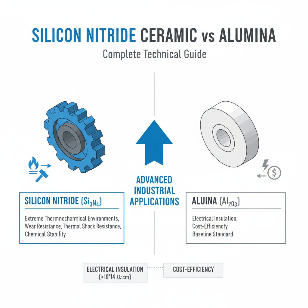
다음에 비해 알루미나/”>알루미나, 실리콘 카바이드는 열전도율과 경도가 매우 우수합니다. 알루미나는 비용 효율성이 높고 전기 절연체 역할을 잘 수행하지만 열전도율이 낮기 때문에(25-35W/m-K) 씰 인터페이스에서 마찰 열이 급증하면 열충격 고장에 취약합니다. 또한 알루미나의 경도는 1500 HV로 상당히 낮아 화학적-기계적 연마(CMP) 도구와 같은 마모성 슬러리 환경에서 마모 속도가 더 빠릅니다.
다음에 대해 평가할 때 지르코니아, 와는 열 관리 측면에서 더욱 뚜렷한 대조를 이룹니다. 지르코니아는 파단 인성(최대 10.0MPa-m½)이 뛰어나 기계적 충격에 매우 강한 것으로 유명합니다. 그러나 지르코니아는 전도율이 2~3W/m-K에 불과한 단열재 역할을 합니다. 고속 메카니컬 씰 애플리케이션에서 지르코니아를 사용하면 씰링 면에 마찰 열을 정확하게 가두어 유체 기화, 열 팽창을 일으킬 수 있습니다. 그리고 치명적인 씰링 실패를 초래할 수 있습니다. 실리콘 카바이드의 열 전도성은 이 열을 중요한 인터페이스에서 적극적으로 제거합니다.
마지막으로, 다음과 비교하면 실리콘 질화물, 실리콘 질화물이 파괴 인성이 약간 더 우수하지만 절대 경도와 열 전도성에서는 여전히 SiC가 우위를 점하고 있습니다. 실리콘 질화물은 높은 기계적 하중을 받는 베어링 볼 및 구조 부품에 탁월한 소재이지만 최대 경도와 열 방출이 성공 요인이 되는 마찰 밀봉 인터페이스의 특정 요구 사항에는 전자제품용 실리콘 카바이드 세라믹 씰 링이 여전히 최고의 엔지니어링 선택입니다.
애플리케이션
독특한 마찰, 열. 그리고 전자제품용 실리콘 카바이드 세라믹 씰 링의 화학적 특성으로 인해 반도체 팹 및 전자 부품 제조 공장 내 가장 혹독한 운영 환경에서도 사용할 수 있습니다. 엔지니어들은 금속 씰이 부식되고 폴리머 씰이 녹을 때 이 정확한 재료를 지정합니다. 그리고 표준 산화물 세라믹은 열 충격을 받으면 균열이 생깁니다.
- 화학적 기계 연마(CMP) 장비 씰: CMP 공정에서 실리콘 웨이퍼는 실리카 또는 세리아 나노 입자가 포함된 고마모성, 화학 반응성 슬러리를 사용하여 평탄화됩니다. 금속 씰은 빠르게 마모되어 미립자 오염 물질을 웨이퍼에 흘려보냅니다. 실리콘 카바이드 씰 링을 선택하는 이유는 2500 HV 이상의 경도가 연마 슬러리에 완벽하게 저항하고 화학적 불활성이 연마 산과의 반응을 방지하여 무결점 웨이퍼 처리를 보장하고 씰 수명을 몇 주에서 몇 달로 연장하기 때문입니다.
- 플라즈마 에칭 챔버 정적 씰: 반도체 제조의 건식 에칭은 고진공 상태에서 작동하는 공격적인 할로겐 플라즈마(예: 불소 또는 염소)를 사용합니다. 이러한 조건에서 폴리머 씰은 분해되고 가스를 배출하여 진공을 파괴하고 유기 오염 물질을 침착시킵니다. 전자제품용 실리콘 카바이드 세라믹 씰 링은 할로겐 플라즈마 침식에 근본적으로 영향을 받지 않고 10-⁸ Torr 진공에서 가스를 배출하지 않기 때문에 사용됩니다. 또한 열악한 챔버 환경에서도 미크론 이하의 치수 안정성을 유지합니다.
- 고전력 마이크로일렉트로닉스를 위한 액체 냉각 시스템 펌프: 데이터센터 서버와 고전력 IGBT 모듈에는 유전체 유체를 사용하는 폐쇄 루프 액체 냉각이 필요합니다. 이러한 냉각 루프를 구동하는 기계식 펌프 씰은 수년 동안 5000~8000RPM으로 지속적으로 작동해야 합니다. 이러한 로터리 씰에는 높은 열 전도성(150W/m-K)으로 마찰 열을 즉시 방출하는 SiC가 선택됩니다. 또한 낮은 마찰 계수는 전력 소모를 최소화하는 동시에 서버 랙에서 유전체 냉각수의 치명적인 누출을 방지합니다.
- MOCVD 서셉터 샤프트 로터리 씰: LED 및 첨단 RF 전자제품 제조에 사용되는 금속-유기 화학 기상 증착(MOCVD) 시스템은 독성 전구체 가스를 주입하면서 1000°C 이상의 온도에서 작동합니다. 웨이퍼 감응체를 회전시키는 회전축에는 동적 씰이 필요합니다. 실리콘 카바이드는 스테인리스 스틸이 휘어지고 PTFE가 즉시 증발하는 온도인 1200°C에서 기계적 강도와 완벽한 밀봉 구조를 유지하기 때문에 선택되었습니다.
- 초순수(UPW) 시스템 씰: 반도체 제조에는 수백만 갤런의 18.2mΩ-cm의 초순수가 필요합니다. 표준 금속 씰은 철, 니켈 또는 크롬 이온을 물로 침출하여 저항을 파괴합니다. 실리콘 카바이드 씰 링은 유체 흐름에 이온을 전혀 침출하지 않기 때문에 UPW 순환 펌프에 사용됩니다. 이 소재의 조밀하고 비다공성 미세 구조는 팹의 용수 공급에 미량 금속 오염 물질을 기여하지 않고 완벽한 봉쇄를 보장합니다.
제조 프로세스
원재료인 화학 분말을 전자제품용 정밀한 실리콘 카바이드 세라믹 씰 링으로 변환하는 것은 복잡한 다단계 엔지니어링 작업입니다. 이 공정에는 엄격한 환경 제어와 정밀하게 프로그래밍된 열 주기가 필요합니다. 그리고 최종 치수를 달성하기 위한 고급 가공 기술도 필요합니다. 표준 산업용 세라믹과 전자 등급 세라믹의 차이점은 전체 제조 수명 주기 동안 순도와 미세 공차에 대한 절대적인 제어에 있습니다.
형성 방법
제조 과정은 초고순도 알파-실리콘 카바이드 분말로 시작되며, 일반적으로 Acheson 공정을 통해 합성된 후 0.5마이크로미터 미만의 D50 입자 크기 분포를 달성하기 위해 정제됩니다. 전자 애플리케이션의 경우 미량 금속 불순물을 10억분의 1(ppb) 수준으로 줄여야 합니다. 이 분말은 임시 유기 바인더 및 윤활제와 균일하게 혼합됩니다.
- 냉간 등방성 프레싱(CIP): 고성능 씰 링의 경우 CIP가 선호되는 성형 방법입니다. 분말을 유연한 탄성체 몰드에 넣고 200~300MPa 범위의 다방향 수압을 가합니다. 이를 통해 그린 바디 전체에 걸쳐 완전히 균일한 밀도 분포를 보장합니다. 이는 소성 단계에서 이방성 수축과 왜곡을 방지하는 데 매우 중요합니다.
- 드라이 프레싱: 더 얇고 부피가 큰 씰링 링의 경우 자동화된 일축 건식 프레스가 사용됩니다. 파우더는 100~150MPa의 압력에서 정밀한 강성 다이로 압축됩니다. 더 빠르고 경제적이지만 씰링 높이 전체에 걸친 밀도 구배를 관리하려면 신중한 다이 설계가 필요합니다.
소결
성형 후 녹색 부품은 400~600°C에서 세심한 바인더 번아웃 단계를 거쳐 미세 균열을 유발하지 않고 모든 유기 첨가제를 제거합니다. 그런 다음 부품은 소결을 위해 고진공 또는 아르곤 분위기의 용광로로 옮겨집니다. 소결 방법은 전자기기용 실리콘 카바이드 세라믹 씰 링의 최종 특성에 큰 영향을 미칩니다.
For Sintered Silicon Carbide (SSiC), the furnace is ramped to extreme temperatures between 2100°C and 2200°C. Small additions of boron and carbon act as sintering aids. During this process, the material undergoes a volumetric shrinkage of 15% to 20%, densifying to over 98% of its theoretical maximum density. The resulting microstructure is entirely single-phase, containing no free silicon, granting it maximum chemical resistance to HF and HNO3 acids. Alternatively, Reaction Bonded Silicon Carbide (RBSiC) is sintered at lower temperatures (circa 1500°C) by infiltrating a porous SiC/carbon preform with molten silicon. While RBSiC exhibits near-zero shrinkage, the presence of free silicon makes it less suitable for ultra-aggressive electronics etching environments than pure SSiC.
최종 가공
Because SSiC shrinks by up to 20% during sintering, the “as-fired” component cannot meet the strict dimensional requirements of the electronics industry. This often dictate geometric tolerances measured in micrometers. Final machining is the most critical and cost-intensive phase of production. Because the material hardness exceeds 2500 HV, traditional carbide or high-speed steel tools are completely ineffective. they will instantly dull or shatter upon contact.
The seal rings must be shaped using state-of-the-art CNC grinding centers equipped with resin-bonded or metal-bonded diamond abrasive wheels. The process involves rough grinding to establish the outer and inner diameters, followed by precision face grinding. For a mechanical seal ring, the mating face must be extremely flat to prevent fluid leakage at the micro-level. This requires specialized lapping machines utilizing diamond slurries (typically 1 to 3-micron grit) on cast iron or composite plates, followed by a final polishing stage. 정밀 세라믹 가공 techniques are employed to achieve surface finishes of Ra < 0.1 µm and flatness levels better than 1 light band (0.29 µm). If you are looking for a reliable manufacturing partner capable of executing these exacting operations, ensure they possess comprehensive metrology laboratories to verify every single tolerance.
장점 및 제한 사항
Selecting a silicon carbide ceramic seal ring for electronics requires a balanced understanding of its engineering profile. While it solves many catastrophic failure modes associated with metals and plastics, it introduces specific design constraints that mechanical engineers must accommodate.
장점
- 탁월한 내마모성: The 2500-2800 HV hardness rating ensures that the seal face undergoes practically zero wear over tens of thousands of operational hours, drastically increasing the MTBF of semiconductor processing equipment and reducing maintenance downtime.
- Superior Thermal Management: Operating at 120-150 W/m·K, the material acts as its own heat sink. In high-velocity rotary applications within electronics cooling loops, it pulls destructive frictional heat away from the dynamic sealing interface, preventing the thermal breakdown of adjoining elastomers.
- Absolute Chemical Inertness: In the harsh chemical environments of wafer fabrication—involving hydrofluoric acid, sulfuric acid. And fluorine plasmas—SSiC remains completely unreactive. It will not dissolve, pit, or release particulate contamination into the pure processing stream.
- Dimensional Stability under Thermal Stress: With a coefficient of thermal expansion (CTE) of approximately 4.0 x 10⁻⁶ /°C (less than half that of steel), SiC seal rings maintain precise interference fits and micron-level flatness profiles even when equipment rapidly cycles from room temperature to hundreds of degrees Celsius.
제한 사항
- 내재된 취성: Like all advanced ceramics, silicon carbide has a relatively low fracture toughness (4.0 – 4.5 MPa·m½). It is highly susceptible to brittle fracture if subjected to sudden mechanical impact, high-stress concentrations from sharp corners, or improper assembly techniques. Engineering designs must avoid point loads and incorporate chamfers or radii.
- High Manufacturing and Machining Costs: The necessity of processing temperatures exceeding 2100°C and the absolute requirement for diamond-tooled precision grinding makes SiC components significantly more expensive to produce than metal or alumina equivalents. However, the total cost of ownership (TCO) is heavily offset by the exponential increase in component lifespan.
가공 고려 사항
Producing a silicon carbide ceramic seal ring for electronics that meets the uncompromising standards of the semiconductor industry presents severe machining challenges. The very property that makes SiC desirable—its immense hardness—makes it notoriously difficult to cut, drill, or grind. When machining a material this hard, engineers battle constantly against rapid tool wear, the introduction of sub-surface micro-cracks. And edge chipping. The cutting parameters must be aggressively controlled to prevent inducing thermal and mechanical stresses into the brittle ceramic matrix.
To demonstrate the level of precision and deterministic machining required, the table below outlines typical high-end machining tolerances that expert ceramic manufacturers must achieve for electronics-grade seal rings:
| 가공 매개변수 | 표준 허용 오차 | Great Ceramic 정밀도 |
|---|---|---|
| 외경/내경(OD/ID) | ±0.05 mm | ±0.005 mm |
| 동심도 | 0.02 mm | 0.005 mm |
| Surface Finish (Ra) | 0.4 µm | < 0.1 µm |
| Flatness (Sealing Face) | 3 Light Bands (~0.9 µm) | 1 Light Band (< 0.3 µm) |
At Great Ceramic, overcoming these challenges is our core competency. Achieving tight tolerances of ±0.005mm on a silicon carbide ceramic seal ring for electronics requires rigid, vibration-damped CNC machine tools and optimized kinematic programming. Spindle speeds, feed rates (often restricted to a few millimeters per minute). And depths of cut (frequently sub-millimeter) are meticulously calculated. High-pressure, temperature-controlled flood coolant is directed precisely at the grinding zone to flush away abrasive swarf and prevent localized thermal shock from the friction of the diamond wheel.
Furthermore, edge chipping is mitigated through specialized toolpath strategies, such as climb grinding and the implementation of sacrificial backing materials during through-hole generation. The lapping process, essential for achieving a flatness of less than 1 light band, requires continuous monitoring of the lapping plate’s curvature and precise dosing of the diamond slurry suspension. Our metrology department employs advanced Coordinate Measuring Machines (CMM), laser interferometers. And optical profilometers to validate that every single geometric callout on the engineering drawing is met to the exact micron.
FAQ
What is a silicon carbide ceramic seal ring for electronics?
A silicon carbide ceramic seal ring for electronics is a highly engineered mechanical component used to create a leak-proof barrier in dynamic (rotating) or static environments within semiconductor and microelectronics manufacturing equipment. Constructed from ultra-high purity alpha-silicon carbide powder sintered at extreme temperatures, this component exhibits extraordinary hardness, exceptional thermal conductivity. And absolute chemical inertness. It is specifically designed to operate in severe environments—such as high-speed pumps for dielectric coolants, aggressive CMP slurry dispensing. And vacuum plasma etching chambers—where traditional metal, polymer, or lower-grade ceramic seals would rapidly fail due to wear, thermal degradation, or corrosive attack. The component ensures zero contamination and maintains tight dimensional stability under stress.
What are the main applications of a silicon carbide ceramic seal ring for electronics?
The main applications revolve around semiconductor wafer fabrication and high-power electronic cooling infrastructure. They are predominantly utilized as dynamic mechanical seal faces in pumps that circulate ultra-pure water (UPW) or dielectric liquid coolants for data centers and IGBT modules, where rapid heat dissipation and low friction are mandatory. Additionally, they serve as retaining rings and seals in Chemical Mechanical Polishing (CMP) equipment, resisting the highly abrasive nanoparticle slurries. They are also deployed as static structural seals in plasma etching and Metal-Organic Chemical Vapor Deposition (MOCVD) reactors, where the material’s resistance to halogen gases, extreme vacuum stability. And ability to withstand temperatures over 1000°C without warping or outgassing are critical for defect-free microchip production.
How does a silicon carbide ceramic seal ring for electronics compare to other ceramics?
When compared to other industrial ceramics, a silicon carbide ceramic seal ring for electronics stands out primarily due to its superior thermal conductivity (120-150 W/m·K) and hardness (2500-2800 HV). For instance, while 알루미나 is widely used due to its low cost and excellent electrical insulation, its low thermal conductivity (25-35 W/m·K) makes it prone to thermal shock and failure in high-speed mechanical seal applications. 지르코니아 offers unparalleled fracture toughness, making it highly impact-resistant, but its extremely low thermal conductivity (2-3 W/m·K) makes it entirely unsuitable for dissipating frictional heat in rotary seals. While 실리콘 질화물 provides a good balance of strength and thermal shock resistance, silicon carbide remains the undisputed leader for tribological sealing faces requiring absolute maximum hardness, wear resistance. And heat dissipation.
What are the advantages of a silicon carbide ceramic seal ring for electronics?
The primary advantages are rooted in its ability to dramatically extend the Mean Time Between Failures (MTBF) in critical manufacturing equipment. Its hardness of over 2500 HV guarantees an exceptionally low wear rate, ensuring that the seal geometry remains perfectly flat over millions of rotational cycles. The material’s high thermal conductivity prevents localized heat buildup, safeguarding adjacent elastomer components from thermal degradation. Furthermore, Sintered Silicon Carbide (SSiC) is completely chemically inert to nearly all acids, alkalis. And etching plasmas used in electronics manufacturing, meaning it will not corrode or release trace metal contaminants (ions or particulates) into ultra-pure processing environments. Finally, its low coefficient of thermal expansion ensures micron-level dimensional stability despite severe temperature fluctuations.
How is a silicon carbide ceramic seal ring for electronics machined?
Machining a silicon carbide ceramic seal ring for electronics is a complex subtractive manufacturing process that occurs entirely after the material has been sintered to its full hardness. Because SiC is harder than tungsten carbide or tool steel, it cannot be turned or milled using traditional methods. Instead, it must be ground using precision CNC machining centers equipped with industrial diamond-impregnated abrasive wheels. The process requires highly rigid machines, optimized feed rates. And high-pressure coolant to prevent edge chipping and subsurface micro-cracking. To achieve the requisite sealing face flatness (often less than 0.3 micrometers or 1 light band) and ultra-smooth surface finishes (Ra < 0.1 µm), the rings undergo specialized multi-stage lapping and polishing processes using progressively finer diamond slurries. At Great Ceramic, our advanced 정밀 세라믹 가공 capabilities and strict metrology protocols ensure we reliably achieve tight tolerances of ±0.005mm on complex SiC geometries.
Need custom silicon carbide ceramic seal ring for electronics parts? 그레이트 세라믹에 문의 공차가 엄격한 정밀 가공 서비스 또는 이메일 [email protected].
전자제품용 실리콘 카바이드 세라믹 씰 링은 고급 세라믹 애플리케이션에 널리 사용됩니다.
자세히 알아보기 전자제품용 실리콘 카바이드 세라믹 씰링 정밀 세라믹 가공 서비스를 제공합니다.