nitreto de alumínio ceramic plate for semiconductor: Complete Technical Guide
The continuous scaling of semiconductor nodes below 5nm has introduced unprecedented thermal management challenges. As power densities in modern microprocessors and insulated-gate bipolar transistors (IGBTs) exceed 1,000 W/cm², traditional substrate materials rapidly fail to dissipate heat efficiently. An aluminum nitride ceramic plate for semiconductor applications serves as the ultimate engineering solution to this bottleneck. By combining a theoretical thermal conductivity exceeding 320 W/m·K (with practical commercial yields of 170-230 W/m·K) and exceptional dielectric strength (up to 15 kV/mm), this advanced material acts as both an electrical insulator and a highly efficient thermal conductor. Furthermore, its coefficient of thermal expansion (CTE) of 4.5 ppm/K closely matches that of silicon (4.0-4.2 ppm/K at 200°C), virtually eliminating thermal stress fractures during high-frequency thermal cycling. For engineers struggling with thermal runaway, dielectric breakdown, or wafer contamination, integrating these plates is no longer optional—it is a baseline requirement. If your current project demands tight-tolerance thermal management solutions, explore our maquinagem de precisão em cerâmica services to achieve ±0.005mm accuracy on your next prototype.
Propriedades do material
The exceptional performance of an aluminum nitride (AlN) plate stems from its covalent bonding and wurtzite crystal structure. In semiconductor manufacturing, heat is primarily transferred via lattice vibrations (phonons). Unlike oxides where oxygen atoms scatter phonons, high-purity AlN minimizes structural defects, allowing thermal energy to travel with minimal resistance. A reduction of oxygen impurities from 1.0% to 0.1% can increase thermal conductivity by nearly 40%. Below is the standard technical data for semiconductor-grade AlN components operating in ultra-high vacuum (UHV) and high-temperature environments.
| Imóveis | Valor | Unidade |
|---|---|---|
| Densidade | 3.26 - 3.30 | g/cm³ |
| Dureza | 1100 - 1200 | HV |
| Resistência à flexão | 300 - 400 | MPa |
| Resistência à fratura | 2.6 – 3.5 | MPa-m½ |
| Condutividade térmica | 170 – 230 | W/m-K |
| Resistividade eléctrica | > 10¹⁴ | Ω-cm |
| Temperatura máxima de funcionamento | 1000 (Ar) / 1900 (Inerte) | °C |
Comparação com outras cerâmicas
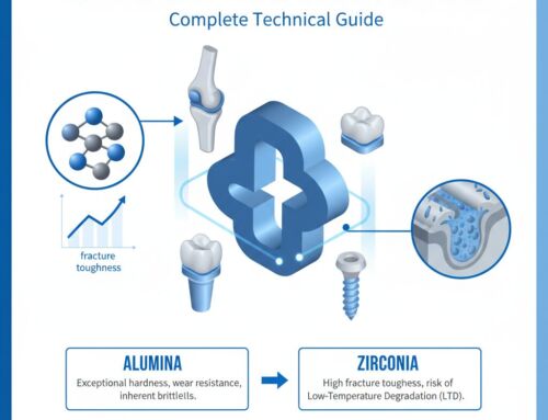
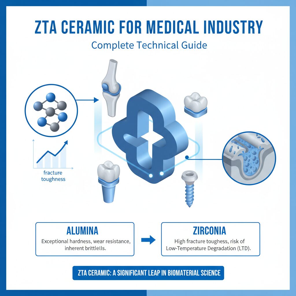
Selecting the optimal substrate requires a data-driven evaluation of competing advanced ceramics. While alumina/”>alumina remains the industry standard for general-purpose electronics due to its low cost and ease of manufacturing, its thermal conductivity caps at roughly 35 W/m·K. This is 85% lower than AlN. This makes alumina fundamentally unsuitable for high-power semiconductor packaging. Conversely, zircónia offers unparalleled fracture toughness (up to 10.0 MPa·m½), making it ideal for structural wear parts, but it acts as a thermal insulator (2-3 W/m·K). This would cause immediate thermal runaway in a semiconductor die. Nitreto de silício represents the closest competitor, offering exceptional mechanical strength (800 MPa) and a high fracture toughness (6.0-8.0 MPa·m½), but its standard thermal conductivity (30-90 W/m·K) still falls significantly short of an aluminum nitride ceramic plate for semiconductor systems.
| Imóveis | aluminum nitride ceramic plate for semiconductor | Alumina (99,5%) | Zircónio (Y-TZP) | Nitreto de silício (Si3N4) |
|---|---|---|---|---|
| Condutividade térmica | 170 – 230 W/m·K | 25 – 35 W/m·K | 2 – 3 W/m·K | 30 – 90 W/m·K |
| Dureza | 1100 – 1200 HV | 1500 – 1650 HV | 1200 – 1300 HV | 1400 – 1600 HV |
| Resistência à fratura | 2.6 – 3.5 MPa·m½ | 3.5 – 4.5 MPa·m½ | 8.0 – 10.0 MPa·m½ | 6.0 – 8.0 MPa·m½ |
| Custo | Elevado | Baixa | Médio | Elevado |
Aplicações
- Electrostatic Chucks (ESCs): In semiconductor etching and deposition tools, ESCs hold 300mm silicon wafers flat utilizing the Johnsen-Rahbek or Coulombic effect. An aluminum nitride ceramic plate is chosen because its volume resistivity can be precisely tuned (between 10⁸ and 10¹² Ω·cm at 20°C to 200°C) by doping with transition metals. Furthermore, it resists aggressive fluorine-based plasmas (such as CF4 and SF6) with an etch rate of less than 1.5 nm/min, ensuring zero particle contamination and an extended lifespan compared to traditional anodized aluminum chucks.
- Wafer Heaters for CVD and PVD: Chemical Vapor Deposition requires extreme temperature uniformity. AlN plates are used as heater platforms because they can achieve continuous operating temperatures of up to 900°C while maintaining a surface temperature variance of less than ±1.5°C across a 300mm diameter. This is critical because a temperature deviation of just 2.0°C can alter film deposition thickness by over 5%, ruining modern 5nm device yields.
- IGBT Power Module Substrates: Insulated-Gate Bipolar Transistors in electric vehicles and renewable energy grids operate at switching voltages exceeding 1200V and current densities of 400A. Using AlN as a Direct Bonded Copper (DBC) or Active Metal Brazed (AMB) substrate prevents dielectric breakdown due to its 15 kV/mm strength. Its thermal expansion coefficient (4.5 ppm/K) closely matches the silicon die (4.1 ppm/K), meaning the solder joints experience minimal shear stress during thousands of thermal cycles from -40°C to +150°C.
- Optoelectronics and UV-C LED Packaging: Deep ultraviolet LEDs (operating in the 260-280 nm range) suffer from catastrophic efficiency droop if junction temperatures exceed 85°C. Implementing an aluminum nitride ceramic plate as the submount immediately pulls heat away from the multi-quantum well structure. Because AlN possesses a thermal conductivity of 200 W/m·K, it lowers the junction temperature by up to 25°C compared to alumina submounts, thereby increasing the optical power output by over 15% and extending device lifespan past 10,000 hours.
- RF and Microwave Window Components: 5G telecommunication base stations and military radar systems require materials with ultra-low signal attenuation at frequencies between 10 GHz and 100 GHz. AlN exhibits a low dielectric constant (approx. 8.8 at 1 MHz) and an incredibly low dielectric loss tangent (tan δ < 0.0003). This ensures that high-frequency electromagnetic waves pass through the ceramic with less than 0.1 dB insertion loss, while the material simultaneously extracts up to 50W of excess heat generated by the amplifying electronics.
Processo de fabrico
Producing a defect-free aluminum nitride ceramic plate for semiconductor applications requires meticulous control over the entire supply chain, from powder synthesis to final nanoscale polishing. Because oxygen is the primary enemy of AlN’s thermal conductivity, every phase of manufacturing must actively suppress oxidation. At Great Ceramic, our process is optimized to maintain oxygen impurities below 0.1 wt%, ensuring the final product consistently hits the 170-230 W/m·K thermal threshold.
Métodos de moldagem
- Fundição em fita: Ideal for thin-film substrates ranging from 0.15mm to 1.5mm thick. Sub-micron AlN powder (typically d50 = 1.2 µm) is mixed with an organic binder (like polyvinyl butyral), plasticizers. And dispersants in a non-aqueous solvent system (such as toluene/ethanol) to prevent hydrolysis. The resulting slurry is cast under a doctor blade with gap tolerances of ±0.01mm. The green tape is then dried, cut. And stacked for DBC/AMB substrate applications.
- Dry Pressing and Isostatic Pressing: For thick structural components such as 20mm thick electrostatic chucks or wafer heaters, cold isostatic pressing (CIP) is utilized. The AlN powder is spray-dried with 2-3 wt% organic binders to form spherical, flowable granules. These are pressed under multi-axial hydraulic pressures exceeding 200 MPa, achieving a green density of roughly 60% of theoretical, eliminating internal porosity before the high-temperature firing phase.
Sinterização
Because aluminum nitride is a highly covalent compound, standard solid-state sintering is nearly impossible without exceeding 2200°C. Therefore, Liquid Phase Sintering (LPS) is employed. Yttrium oxide (Y2O3) or calcium oxide (CaO) is added as a sintering aid at 3-5 wt%. During sintering in a pure nitrogen atmosphere at 1800°C to 1900°C, the Y2O3 reacts with the unavoidable native alumina (Al2O3) layer on the AlN particles to form a liquid yttrium aluminate phase (such as Y3Al5O12 or YAG). This liquid promotes rapid densification to >99% theoretical density while simultaneously “scavenging” oxygen out of the AlN lattice. This is the primary mechanism that unlocks the material’s massive thermal conductivity. Cooling rates must be strictly maintained at 2-5°C/min to prevent thermal shock.
Maquinação final
The sintered aluminum nitride plate shrinks by approximately 18-20% during firing, meaning post-sintering precision machining is mandatory to achieve semiconductor-grade dimensional accuracy. Using advanced multi-axis CNC grinding centers equipped with resin-bonded diamond wheels (typically D46 to D15 grit sizes), the bulk material is reduced. To achieve the extreme flatness (<0.002mm per 100mm) required for wafer chucks, double-sided planetary lapping is performed using boron carbide or diamond slurries (1-3 µm particle size). For applications requiring zero subsurface damage, chemical-mechanical polishing (CMP) is applied to achieve surface roughness (Ra) values below 0.05 µm. Discover more about our raw material capabilities by reviewing our nitreto de alumínio technical specifications.
Vantagens e limitações
Vantagens
- Gestão térmica excecional: With a thermal conductivity of up to 230 W/m·K, AlN outpaces nearly all other ceramic insulators, transferring heat 5 to 7 times faster than standard 99.5% Al2O3.
- Silicon-Matched CTE: Its coefficient of thermal expansion (4.5 x 10⁻⁶ /°C) is nearly identical to silicon (4.1 x 10⁻⁶ /°C) and gallium arsenide (5.8 x 10⁻⁶ /°C), preventing die-cracking and solder-joint delamination during rapid thermal cycling from 0°C to 200°C.
- Elevada rigidez dielétrica: A breakdown voltage exceeding 15 kV/mm combined with a volume resistivity of >10¹⁴ Ω·cm ensures complete electrical isolation in high-voltage IGBT and MOSFET applications.
- Halogen Plasma Resistance: AlN exhibits near-zero erosion in fluorine and chlorine-based plasma environments, making it chemically stable in severe dry-etching and CVD semiconductor equipment.
Limitações
- Susceptibility to Hydrolysis: Raw AlN powder and unpolished machined surfaces can react with ambient humidity (moisture) to form aluminum hydroxide and release ammonia gas (AlN + 3H2O → Al(OH)3 + NH3). Components must be stored in dry environments or undergo passivation/coating protocols.
- High Manufacturing Costs: The necessity for high-purity raw powders, inert gas sintering atmospheres at 1900°C. And expensive diamond-based machining makes AlN up to 3-5 times more expensive than standard alumina components.
Considerações sobre maquinagem
Achieving an ultra-precise aluminum nitride ceramic plate for semiconductor equipment is notoriously difficult due to the material’s inherent brittleness and high hardness (1100-1200 HV). When engineers specify tolerances of ±0.005mm, standard metalworking techniques instantly fail. The primary failure mode during CNC grinding is brittle fracture. This manifests as micro-chipping at the edges or subsurface damage (SSD) extending up to 50 µm beneath the machined surface. To mitigate this, Great Ceramic employs deterministic micro-grinding within the ductile-brittle transition regime. By maintaining the uncut chip thickness below the critical threshold of 0.2 µm, we ensure material is removed via plastic deformation rather than catastrophic cracking.
| Machining Operation | Tool Material / Grit | Spindle Speed (RPM) | Feed Rate (mm/min) | Achievable Tolerance (mm) |
|---|---|---|---|---|
| Rough Milling / Grinding | Diamond (D64 – D91) | 6,000 – 10,000 | 50 – 150 | ±0.050 |
| Precision Surface Grinding | Resin Bond Diamond (D15) | 12,000 – 18,000 | 10 – 30 | ±0.005 |
| Ultrasonic Drilling | Electroplated Diamond Tube | 20 000 – 30 000 | 2 – 10 | ±0.010 |
| Planetary Lapping | Diamond Slurry (3 µm) | 30 – 60 | N/A | Flatness < 0.002 |
Coolant selection is another critical engineering parameter. Because AlN is prone to hydrolysis when exposed to water, water-based coolants can degrade the surface chemistry and introduce oxygen impurities, subsequently lowering the surface thermal conductivity. We exclusively utilize specialized, low-viscosity, oil-based synthetic coolants delivered at high pressures (up to 50 bar) to flush away abrasive swarf while providing hydrodynamic lubrication. This precise control over thermal loads during machining guarantees that the final ceramic part exhibits a flawless surface finish (Ra < 0.1 µm) without microscopic stress fractures. If your semiconductor design requires complex features like embedded gas channels or multi-stepped electrostatic chuck profiles, we have the specialized equipment to execute it flawlessly. Contact our engineering team to discuss how our maquinagem de precisão em cerâmica can solve your supply chain bottlenecks.
FAQ
What is an aluminum nitride ceramic plate for semiconductor?
An aluminum nitride ceramic plate for semiconductor is a highly specialized, non-oxide advanced ceramic substrate designed specifically for microelectronics and wafer processing equipment. It is engineered to provide simultaneous electrical insulation (dielectric strength of 15 kV/mm) and exceptional heat dissipation (thermal conductivity of 170-230 W/m·K). These plates are used as foundational building blocks for components like electrostatic chucks, wafer heaters. And IGBT power modules, where efficiently extracting heat from densely packed silicon or carboneto de silício dies is critical to preventing thermal runaway and device failure.
What are the main applications of an aluminum nitride ceramic plate for semiconductor?
The primary applications revolve around thermal management and plasma resistance in semiconductor fabs. Major uses include Electrostatic Chucks (ESCs) that grip 300mm wafers via high-voltage fields. wafer heater pedestals that operate up to 900°C with extreme ±1.5°C temperature uniformity. Direct Bonded Copper (DBC) substrates for high-power IGBT/MOSFET modules in electric vehicles. and submounts for high-power optoelectronics like deep UV-C LEDs and laser diodes. They are also highly valued as RF microwave windows due to their low dielectric loss of less than 0.0003.
How does an aluminum nitride ceramic plate for semiconductor compare to other ceramics?
Compared to standard 99.5% alumina (Al2O3), an AlN plate offers 5 to 7 times higher thermal conductivity (170+ W/m·K vs 35 W/m·K) and a significantly better CTE match with silicon (4.5 ppm/K vs 7.2 ppm/K). This eliminates thermal cycling stress. While zirconia provides vastly superior fracture toughness (up to 10 MPa·m½ compared to AlN’s 3.0 MPa·m½), zirconia is a thermal insulator and cannot be used for heat dissipation. Silicon nitride matches AlN in CTE and surpasses it in mechanical strength, but its thermal conductivity typically caps at 90 W/m·K, making AlN the undisputed choice for peak thermal transfer.
What are the advantages of an aluminum nitride ceramic plate for semiconductor?
The greatest advantage is the dual-functionality of massive thermal conductivity combined with strict electrical isolation. This allows engineers to mount electrically active, high-heat dies directly onto the substrate without intermediate insulating layers that would otherwise bottleneck heat flow. Secondary advantages include its closely matched coefficient of thermal expansion (CTE) with silicon and gallium arsenide. This prevents solder fatigue. Finally, its chemical inertness to highly aggressive halogen plasmas (like CF4/O2 mixtures used in dry etching) ensures extended component life and zero heavy-metal particle contamination in a cleanroom environment.
How is an aluminum nitride ceramic plate for semiconductor machined?
Machining an aluminum nitride plate to semiconductor-grade tolerances requires rigorous, deterministic micro-grinding techniques to overcome the material’s extreme hardness (1200 HV) and brittleness. At Great Ceramic, we utilize multi-axis, rigid CNC grinding centers equipped with high-concentration, resin-bonded diamond tooling. Spindle speeds exceed 15,000 RPM while maintaining ultra-low feed rates to keep cut-depths in the ductile regime (<0.2 µm), preventing subsurface micro-cracking. Post-grinding, the plates undergo double-sided planetary lapping and CMP polishing to achieve Ra < 0.1 µm finishes and extreme flatness (<0.002mm/100mm). To avoid the material's tendency for hydrolysis, we employ specialized non-aqueous, oil-based coolants during all wet-machining phases.
Need custom aluminum nitride ceramic plate for semiconductor parts? Contactar Great Ceramic para serviços de maquinagem de precisão com tolerâncias apertadas, ou envie um e-mail para [email protected].
aluminum nitride ceramic plate for semiconductor is widely used in advanced ceramic applications.
Saiba mais sobre Aluminum Nitride Ceramic Plate For Semiconductor e os nossos serviços de maquinagem de precisão em cerâmica.