Applications of Advanced Ceramics in the Semiconductor & Electronic

indústria eletrónica

The semiconductor and electronic components industry demands materials that can operate reliably under extreme conditions—high temperatures, rapid thermal cycling, high voltages, and ultra-clean manufacturing environments. Advanced ceramics have become indispensable in this field due to their exceptional combination of mechanical strength, electrical insulation, thermal stability, and chemical inertness. Materials such as alumina (Al₂O₃), nitreto de alumínio (AlN), nitreto de silício (Si₃N₄), zircónia (ZrO₂), beryllium oxide (BeO), e nitreto de boro (BN) are widely used in semiconductor processing equipment, microelectronic packaging, and high-performance electronic devices.

Key Advantages of Advanced Ceramics for Semiconductor & Electronics Applications

Ceramics such as alumina and aluminum nitride have dielectric strengths exceeding 10 kV/mm, making them ideal for use as insulators in high-voltage circuits e substrates for microchips. Their ability to prevent electrical leakage ensures signal integrity in high-speed electronics.

Aluminum nitride and beryllium oxide exhibit outstanding thermal conductivity (AlN: ~170–200 W/m·K; BeO: ~200–250 W/m·K), enabling efficient heat dissipation in power semiconductors, LED modules, e RF devices. This prevents overheating and extends device lifespan.

Advanced ceramics maintain their shape and performance in temperatures ranging from cryogenic levels up to over 1,000°C. This is essential for semiconductor fabrication equipment, where precise tolerances are crucial for lithography, etching, and deposition processes.

Semiconductor manufacturing often involves aggressive chemicals and plasma environments. Materials like silicon nitride and alumina resist etchants, acids, and reactive gases, ensuring long component lifetimes in plasma etchers, CVD reactors, and wafer handling systems.

Many ceramics, especially silicon nitride, have low coefficients of thermal expansion, reducing thermal stress during rapid temperature changes and making them compatible with various semiconductor materials.

benefício:

  • Superior Reliability: Stable under high temperatures and voltage stress
  • Enhanced Miniaturization: Enables compact, high-performance designs
  • Improved Thermal Management: Prevents overheating in power electronics
  • Hermetic Sealing Capability: Protects sensitive semiconductor components from moisture and contaminants
  • High Frequency Performance: Low dielectric loss materials for 5G and radar systems

Key Materials in Semiconductor & Electronics Applications

At Great Ceramic, we are committed to advancing the application of high-performance ceramics in the semiconductor and electronics industries, helping our customers achieve unprecedented levels of performance, reliability, and sustainability.

Material Core Properties Aplicações típicas
Alumina (Al₂O₃) Cost-effective, good insulation, moderate thermal conductivity LED substrates, multilayer packages, ceramic PCBs
Nitreto de alumínio (AlN) High thermal conductivity, electrical insulation, CTE match with Si Power module substrates, RF device heat spreaders
Nitreto de silício (Si₃N₄) High fracture toughness, thermal shock resistance Wafer handling arms, power electronic substrates
Carbureto de silício (SiC) High strength, corrosion resistance, thermal stability CVD chamber components, diffusion furnace liners
Nitreto de boro (BN) Thermal conductor + electrical insulator, machinable Heat sinks for RF/microwave devices, interface layers
Cerâmica de vidro maquinável (MGC) Easy precision machining, stable up to 1000°C Prototyping parts, small-batch precision components
ZTA (Alumina endurecida com zircónio) High wear resistance, improved fracture toughness Precision guides, semiconductor handling tools

Performance Advantages Over Metals and Plastics

Imóveis Cerâmica avançada Metais Plásticos
Condutividade térmica High (AlN up to 260 W/m·K) Moderate (Cu: ~400 W/m·K) Low (<1 W/m·K)
Isolamento elétrico Excellent (>10¹³ Ω·cm) Pobres Bom
Resistência à corrosão Excelente Moderate/Poor Bom
Estabilidade a altas temperaturas Excellent (>1000°C) Good (500–800°C) Poor (<200°C)
Resistência ao desgaste Excelente Bom Pobres

Principais aplicações
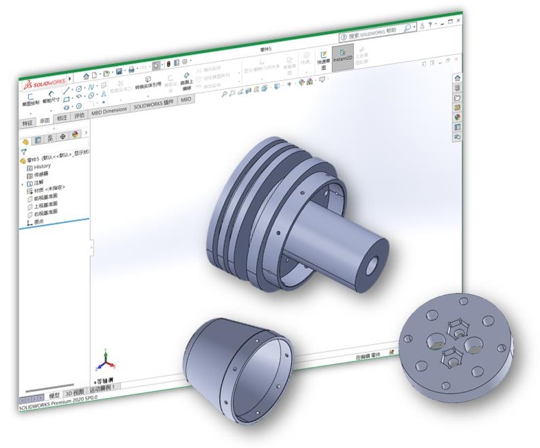
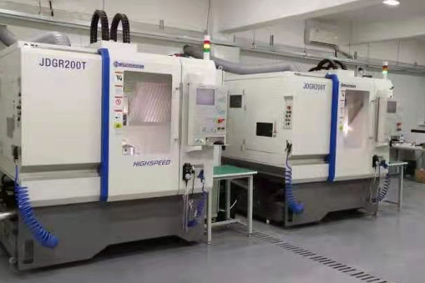
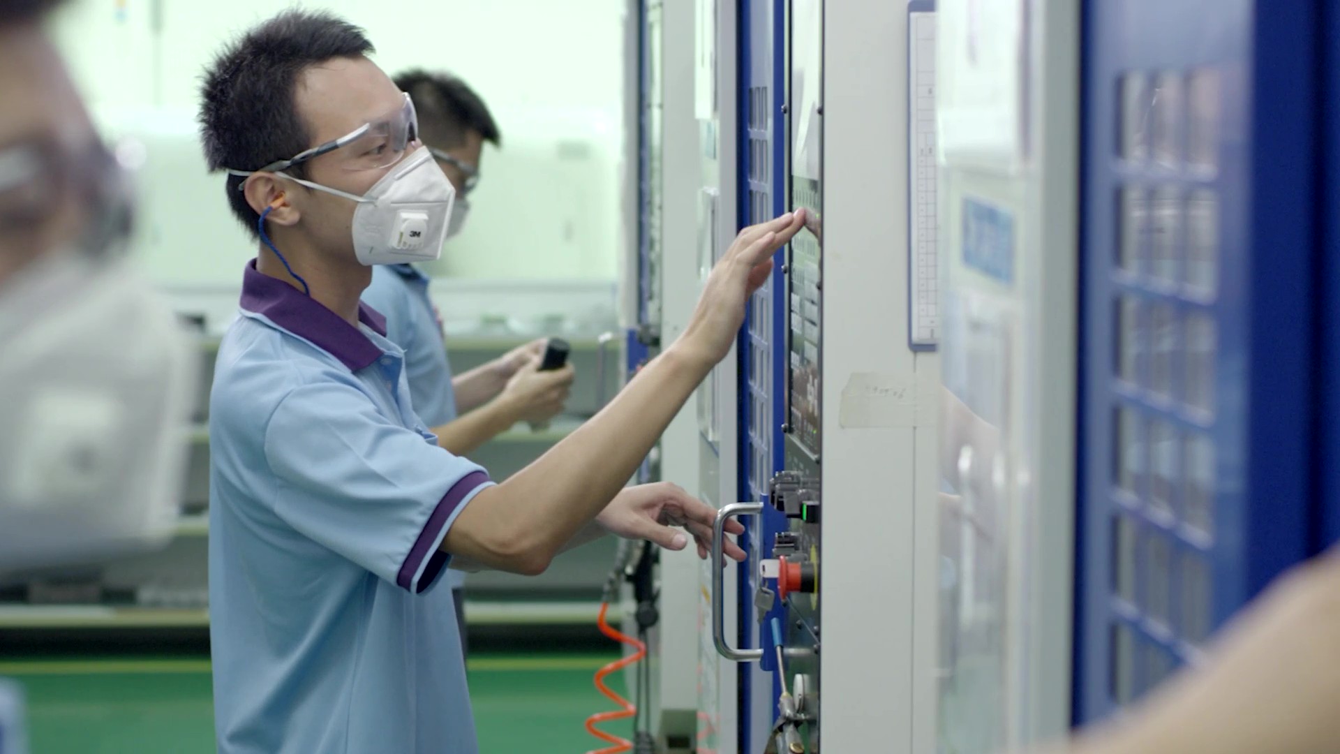
  • AlN ceramic substrates em power modules (IGBT, MOSFET) for electric vehicles and renewable energy systems.

  • DBC/AMB substrates combining ceramics with copper layers for superior heat dissipation.

  • LED packaging: Al₂O₃ for cost-effective general lighting, AlN for UV and high-power LEDs.

  • 5G RF modules: Low-loss ceramics reduce signal attenuation in high-frequency transmission.

  • Si₃N₄ and SiC for wafer handling arms, etching chamber components, and CMP (Chemical Mechanical Planarization) parts.

  • BN as heat shields and susceptor liners in MOCVD systems.

  • Al₂O₃ for plasma-resistant nozzles and insulators.

  • Extended lifetime in harsh process environments reduces maintenance downtime.

  • LTCC (Low-Temperature Co-Fired Ceramic) substrates for compact RF and microwave modules.

  • MLCC (Multilayer Ceramic Capacitors) based on BaTiO₃ for filtering and energy storage.

  • Dielectric resonators and antennas for 5G base stations and radar systems.

  • MGC and ZTA for wafer alignment fixtures and positioning tools.

  • Custom ceramic machining for high-precision robotic arms in pick-and-place systems.

  • Electrostatic chuck (ESC) plates made from high-purity Al₂O₃ for wafer fixation.

Manufacturing Capabilities for Semiconductor-Grade Ceramics

Na Great Ceramic, somos especialistas em maquinagem por medida de componentes cerâmicos avançados. Os nossos serviços de fabrico de precisão garantem que cada peça cumpre as especificações exactas do projeto com tolerâncias apertadas e acabamentos suaves. Oferecemos:
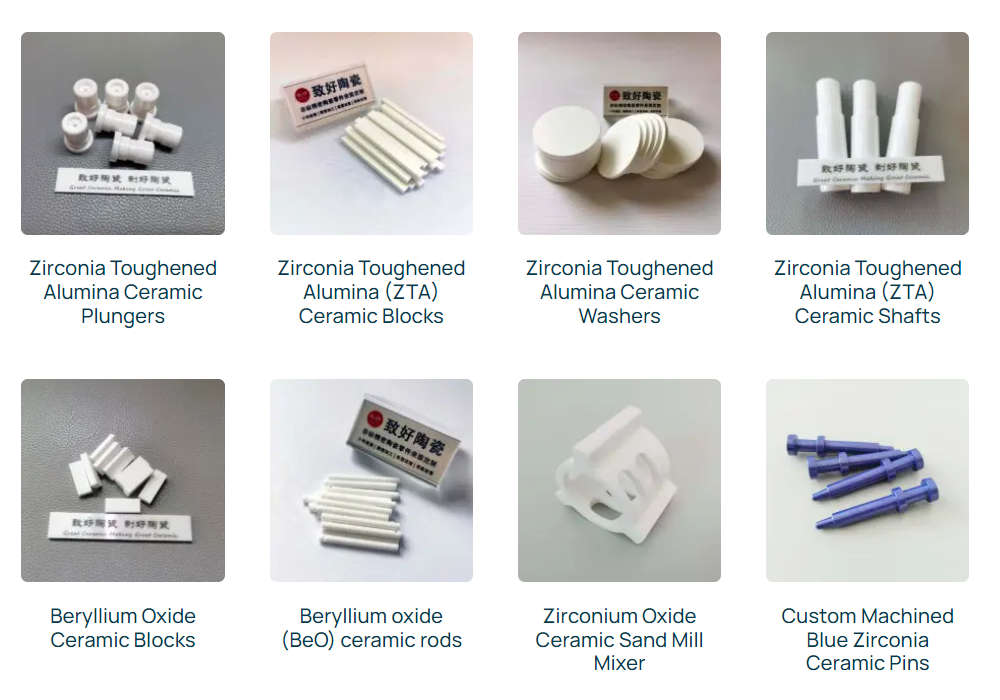
  • Precision CNC machining with tolerances up to ±0.001 mm.
  • Laser micromachining for microvia and complex geometries.
  • Metallization & brazing for hermetic sealing with metals.
  • Rapid prototyping for small-batch R&D components.
  • Surface finishing (polishing, lapping) to sub-micron flatness.

Produtos relevantes

Perguntas frequentes (FAQ)

Aluminum nitride (AlN) and low-loss alumina are most commonly used due to low dielectric loss and good thermal conductivity.

Ceramics combine high thermal conductivity with electrical insulation, eliminating the need for separate insulating layers.

Yes. SiC, Si₃N₄, and high-purity alumina resist plasma gases such as CF₄ and Cl₂ for extended operational lifetimes.

MGCs are ideal for prototyping and small-batch runs but may be replaced by high-performance ceramics for mass production.

AlN has significantly higher condutividade térmica (up to 180 W/m·K), making it more effective for heat dissipation in módulos de potência e RF devices.

Yes, in high-performance applications where heat resistance, electrical insulation, and mechanical stability are crucial, ceramics outperform plastics.

Absolutely. Materials like AlN, Al₂O₃, and Si₃N₄ are widely used in wafer handling, packaging, and substrate manufacturing.

Great Ceramic

Your trusted partner for advanced ceramics

Advanced ceramics are redefining the semiconductor and electronics industries, enabling higher power density, improved thermal management, and longer device life.

Great Ceramic offers precision machining, custom design, and metallization services to meet the demanding requirements of your electronics applications, creating custom, high-performance ceramic components.

Entre em contacto connosco Hoje

Pronto para dar vida aos seus desenhos em cerâmica?
Contacte a Great Ceramic para obter soluções personalizadas de maquinação de cerâmica que satisfaçam os mais elevados padrões da sua aplicação.