Silicon Nitride Ceramic Plate for Semiconductor: Complete Technical Guide
The semiconductor manufacturing industry faces increasingly stringent demands for materials that can withstand extreme environments while maintaining absolute dimensional stability. A silicon nitride ceramic plate for semiconductor applications represents the apex of structural ceramics, offering a critical solution to the industry’s most persistent pain points: thermal stress failure, particulate contamination. And premature component wear. As wafer sizes increase to 300mm and transition toward 450mm, traditional materials experience intolerable deflection and thermal expansion mismatches. Silicon nitride (Si3N4) eliminates these issues by providing an exceptional combination of high fracture toughness (up to 8.0 MPa·m½), a coefficient of thermal expansion (3.2×10⁻⁶/°C) that perfectly mirrors silicon wafers. And extraordinary thermal shock resistance capable of surviving rapid temperature fluctuations exceeding 600°C. This comprehensive technical guide details the mechanical properties, manufacturing methodologies. And advanced machining protocols required to produce these high-purity components with strict tight tolerances of ±0.005mm.
For engineering teams requiring immediate design-for-manufacturability (DFM) feedback, explore our precision ceramic machining capabilities to accelerate your semiconductor equipment prototyping phase.
Material Properties
The operational superiority of a silicon nitride ceramic plate for semiconductor equipment is directly derived from its unique microscopic grain structure. The interlocking needle-like β-Si3N4 grains create a self-reinforcing microstructure that deflects crack propagation. This results in mechanical and thermal properties that consistently outperform conventional cleanroom materials. Below is the rigorously tested empirical data for high-grade sintered silicon nitride used in semiconductor processing environments.
| Property | Value | Unit |
|---|---|---|
| Density | 3.22 – 3.25 | g/cm³ |
| Hardness | 1500 – 1600 | HV |
| Flexural Strength | 800 – 1000 | MPa |
| Fracture Toughness | 6.5 – 8.0 | MPa·m½ |
| Thermal Conductivity | 25.0 – 35.0 | W/m·K |
| Electrical Resistivity | > 10¹⁴ | Ω·cm |
| Max Working Temperature | 1200 – 1400 | °C |
When engineering a silicon nitride ceramic plate for semiconductor applications, density is a critical metric. At 3.22 g/cm³, it is roughly 15% lighter than standard aluminum oxide. This significantly reduces the moment of inertia in dynamic components like wafer handling robots, allowing for acceleration rates exceeding 2G without inducing micro-vibrations. Furthermore, the electrical resistivity of >10¹⁴ Ω·cm ensures absolute dielectric isolation, making it ideal for high-voltage plasma applications in etching chambers where leakage currents must remain below 0.1 microamps.
Comparison with Other Ceramics
Selecting the correct advanced ceramic requires a rigorous comparative analysis of physical properties, thermal behaviors. And lifecycle costs. While silicon nitride represents the premium standard for thermomechanical stability, engineers must evaluate it against other technical ceramics to ensure optimal application alignment.
| Property | Silicon Nitride Plate | Alumina (99.5%) | Zirconia (Y-TZP) | Silicon Carbide |
|---|---|---|---|---|
| Thermal Conductivity | 30.0 W/m·K | 35.0 W/m·K | 2.5 W/m·K | 120.0 W/m·K |
| Hardness | 1500 HV | 1600 HV | 1250 HV | 2500 HV |
| Fracture Toughness | 7.5 MPa·m½ | 4.0 MPa·m½ | 10.0 MPa·m½ | 4.5 MPa·m½ |
| Cost | High | Low | Medium | High |
In high-throughput semiconductor environments, a standard alumina/”>alumina plate is often utilized for basic insulation, but its relatively low fracture toughness (4.0 MPa·m½) makes it highly susceptible to edge chipping during mechanical wafer clamping, generating catastrophic particulate contamination. Conversely, zirconia offers unparalleled fracture toughness (10.0 MPa·m½) but possesses an extremely low thermal conductivity (2.5 W/m·K) and a high coefficient of thermal expansion (10.5×10⁻⁶/°C). This completely disqualifies it from processes requiring rapid thermal cycling or silicon-matching dimensional stability.
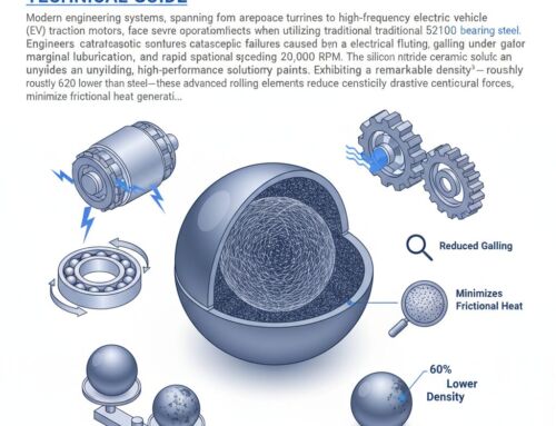
When compared to silicon carbide. This boasts excellent thermal conductivity (120 W/m·K) and extreme hardness (2500 HV), silicon nitride maintains a distinct advantage in fracture toughness and machinability. Silicon carbide’s extreme brittleness (4.5 MPa·m½) makes it highly vulnerable to catastrophic failure from localized mechanical shocks, whereas the interlocking grain structure of a silicon nitride ceramic plate for semiconductor tooling absorbs impact energy, extending the mean time between failures (MTBF) by an average of 400% in dynamic load applications.
Applications
The integration of a silicon nitride ceramic plate for semiconductor manufacturing is pervasive across both Front-End-of-Line (FEOL) and Back-End-of-Line (BEOL) processes. Its deployment is specifically targeted at zones where thermal gradients, corrosive plasmas. And mechanical wear intersect.
- Wafer Heater Chucks (RTP and CVD): In Rapid Thermal Processing (RTP) and Chemical Vapor Deposition (CVD), maintaining uniform wafer temperature is paramount. A silicon nitride plate is utilized as the heating substrate because its thermal expansion perfectly matches the silicon wafer (3.2 ppm/K). This prevents microscopic sliding and backside scratching of the wafer. The material maintains structural rigidity at operating temperatures of 400°C to 800°C, ensuring a flatness deviation of less than 10 micrometers across a 300mm surface. This translates to a thermal uniformity of ±0.5°C.
- CMP Retaining Rings: Chemical Mechanical Planarization (CMP) requires retaining rings that can withstand highly abrasive slurries and strong chemical reagents (pH ranges from 2 to 12). Silicon nitride is chosen for this application because its wear rate is up to 10 times lower than standard polymer rings (like PPS or PEEK) and it will not shed metallic contaminants into the slurry. The high hardness (1500 HV) ensures the ring maintains edge geometry over thousands of polishing cycles, resulting in superior edge-exclusion yields on the polished silicon wafers.
- Wafer Handling End Effectors: High-speed vacuum robot arms must transfer wafers with zero particulate generation and zero deflection. Silicon nitride is selected due to its extraordinary specific stiffness (Young’s modulus to density ratio). Under a standard 2.5 kg payload at maximum robotic acceleration, a 2mm thick silicon nitride end effector exhibits a tip deflection of less than 0.015mm, preventing wafer dropping or misalignment. Additionally, its inherent wear resistance eliminates the generation of micro-dust particles during wafer hand-offs.
- Plasma Etch Chamber Focus Rings: In dry etching processes involving aggressive fluorinated or chlorinated plasmas (e.g., CF4, SF6, Cl2), chamber components face severe chemical degradation and ion bombardment. Silicon nitride ceramic plates are chosen because they exhibit exceptionally low etch rates in halogen plasmas. The high dielectric strength (>15 kV/mm) also ensures proper shaping of the RF electrical fields, directing the plasma uniformly onto the wafer surface without arcing or field distortion.
- Ion Implantation Components: Ion implanters utilize extreme voltages and generate significant localized heat. Silicon nitride insulators and shielding plates are utilized because they do not outgas under ultra-high vacuum (UHV) conditions (10⁻⁸ Torr) and can easily dissipate localized thermal spikes (up to 600°C) without cracking. The high fracture toughness ensures that components bolted into the implanter chassis do not crack under standard torque loads of up to 5 N·m during routine maintenance.
Manufacturing Process
Producing a defect-free silicon nitride ceramic plate for semiconductor applications is a highly engineered, multi-stage metallurgical process. Because pure silicon nitride decomposes at 1850°C before it can melt, it cannot be cast. it must be manufactured using advanced powder metallurgy techniques with specific sintering aids (typically Yttria, Y2O3. And Alumina, Al2O3, at 4-8% total volume) to promote liquid-phase sintering.
Forming Methods
Achieving a homogeneous green body is critical to preventing warping during the densification phase.
- Cold Isostatic Pressing (CIP): For thick plates and complex blanks, silicon nitride powder is sealed in an elastomeric mold and subjected to uniform hydraulic pressure ranging from 200 to 300 MPa. This highly uniform compaction eliminates internal density gradients, yielding a green body with ~60% theoretical density and strictly controlling firing shrinkage to a predictable 18-22%.
- Tape Casting: For ultra-thin plates and substrates (0.2mm to 2.0mm thickness), the ceramic powder is mixed with organic binders and solvents into a slurry. A doctor blade spreads this slurry over a moving carrier belt with a thickness precision of ±0.01mm. The solvent evaporates, leaving a flexible green tape that can be stamped, laser-cut. And laminated before firing.
Sintering
The sintering process is where the critical α-to-β phase transformation occurs, generating the tough, interlocking needle-like grain structure.
Gas Pressure Sintering (GPS) is the dominant method for semiconductor-grade silicon nitride. The green plates are placed in a controlled atmosphere furnace. To suppress the thermal decomposition of Si3N4 into silicon and nitrogen gas at extreme temperatures, the furnace is pressurized with pure Nitrogen gas to levels between 1 MPa and 10 MPa. The temperature is systematically ramped to 1750°C – 1850°C. During this phase, the sintering aids melt, allowing the silicon nitride to dissolve and precipitate out as elongated β-Si3N4 crystals. The result is a fully dense (>99.5%) ceramic matrix completely devoid of internal porosity.
Final Machining
Because the fired plate achieves a hardness of 1500 HV, standard cutting tools cannot penetrate the material. Final machining is executed exclusively using diamond abrasives. The process utilizes multi-axis CNC grinding centers equipped with resin-bonded and metal-bonded diamond wheels. The plate undergoes aggressive rough grinding with 100-grit diamond wheels to establish near-net shape, followed by precision lapping with 3-micron diamond suspensions to achieve the requisite flatness (< 0.005mm) and a surface finish (Ra) of less than 0.1 micrometers.
Advantages & Limitations
Advantages
Deploying a silicon nitride ceramic plate for semiconductor tools provides massive operational advantages that directly translate to increased wafer yield and tool uptime.
- Unmatched Fracture Toughness: At 8.0 MPa·m½, it possesses twice the fracture toughness of alumina. This allows the material to absorb mechanical shocks, torque loads from bolting. And dynamic operational stresses without catastrophic brittle failure or micro-chipping.
- Zero Particulate Generation: The dense, interlocking grain structure results in virtually zero wear under mechanical friction, preventing the generation of microscopic ceramic dust particles that would otherwise contaminate class 10 cleanroom environments and destroy microchip circuitry.
- Thermal Kinematics: With a CTE of 3.2 ppm/K, it mirrors the thermal expansion profile of pure silicon (2.6 – 3.0 ppm/K depending on temperature). When heating a wafer from 20°C to 600°C, the silicon wafer and the silicon nitride plate expand at virtually identical rates, preventing backside scratching and minimizing thermally induced stresses.
- Exceptional Thermal Shock Resistance: Capable of withstanding a sudden temperature differential (ΔT) of over 600°C without cracking, silicon nitride enables rapid heating and cooling cycles in RTP tools, significantly increasing wafer throughput per hour (WPH).
Limitations
Despite its engineering superiority, designers must account for specific limitations when integrating this material into their supply chains.
- High Acquisition Cost: Due to the necessity of high-purity raw powders, complex gas-pressure sintering equipment. And extensive diamond grinding, silicon nitride components can cost 300% to 500% more than equivalent alumina parts. However, the total cost of ownership (TCO) is generally lower due to drastically increased lifespans.
- Extreme Machining Difficulty: The precise attribute that makes it durable—its extreme toughness and hardness—makes it notoriously difficult and time-consuming to machine post-sintering. Generating complex internal geometries or threaded features requires specialized ultrasonic machining or EDM (if electrically conductive dopants are added).
Machining Considerations
The precision machining of a silicon nitride ceramic plate for semiconductor applications represents one of the most formidable challenges in modern industrial manufacturing. Unlike metals that yield and deform under cutting forces, silicon nitride undergoes brittle fracture. If machining parameters are incorrect, the cutting force will induce sub-surface micro-cracks that propagate up to 50 micrometers deep into the material, compromising its structural integrity and causing premature failure in high-stress semiconductor environments.
To overcome this, engineers at Great Ceramic employ “ductile regime grinding.” By strictly limiting the depth of cut to less than 1.0 micrometer per pass, the material is removed via plastic deformation rather than brittle fracture, entirely eliminating sub-surface damage. This requires ultra-rigid CNC machine tools utilizing hydrostatic bearings to prevent spindle runout. Diamond wheel selection is mathematically optimized. we utilize metal-bonded diamond wheels with #120 to #200 grit (grain size 75-125 µm) at spindle speeds of 8,000 to 12,000 RPM for roughing, followed by resin-bonded #800 to #1500 grit wheels for finishing.
Coolant management is equally critical. High-pressure (up to 50 bar) synthetic coolants are directed precisely at the cutting interface to dissipate the massive frictional heat generated, preventing thermal degradation of the diamond tooling. Through these advanced methodologies, Great Ceramic guarantees exceptional precision. The table below outlines our standard and tight-tolerance capabilities for silicon nitride processing.
| Machining Feature | Standard Tolerance | Great Ceramic Tight Tolerance |
|---|---|---|
| Dimensional (L/W/T) | ± 0.050 mm | ± 0.005 mm |
| Flatness (per 100mm) | 0.020 mm | 0.003 mm |
| Parallelism | 0.020 mm | 0.003 mm |
| Surface Finish (Ra) | 0.4 – 0.8 µm | < 0.05 µm (Polished) |
| Hole Diameter | ± 0.050 mm | ± 0.010 mm |
To review our specific spindle speeds, tool path strategies, or to submit an RFQ for tight-tolerance components, consult our comprehensive precision ceramic machining division.
FAQ
What is a silicon nitride ceramic plate for semiconductor?
A silicon nitride ceramic plate for semiconductor manufacturing is a high-purity, structural ceramic component engineered primarily from Si3N4. It is utilized in cleanroom environments for processing silicon wafers. The material is chosen specifically because its coefficient of thermal expansion closely matches that of a silicon wafer, its high fracture toughness (up to 8.0 MPa·m½) prevents particle contamination. And its excellent thermal stability allows it to function flawlessly in etching, deposition. And thermal processing equipment at temperatures up to 1200°C.
What are the main applications of a silicon nitride ceramic plate?
In the semiconductor industry, these plates are primarily used as wafer heater chucks in Chemical Vapor Deposition (CVD) and Rapid Thermal Processing (RTP) tools, where they provide uniform heating across a 300mm surface. They are also used as retaining rings in Chemical Mechanical Planarization (CMP) equipment, as end-effectors on vacuum robotic arms for high-speed wafer handling. And as dielectric focus rings and shields inside highly corrosive dry plasma etching chambers.
How does a silicon nitride ceramic plate compare to other ceramics?
Compared to standard alumina, silicon nitride has double the fracture toughness and infinitely superior thermal shock resistance, allowing it to survive 600°C temperature drops without cracking. Compared to zirconia, silicon nitride possesses a much lower and more stable coefficient of thermal expansion (3.2 ppm/K vs 10.5 ppm/K), making it vastly superior for high-temperature dimensional stability. While silicon carbide offers higher thermal conductivity, silicon nitride is much less brittle, rendering it highly resistant to mechanical impact and edge chipping during continuous wafer processing.
What are the advantages of using silicon nitride in cleanrooms?
The primary advantage is the absolute elimination of particulate contamination. Because silicon nitride has an extremely high hardness (1500 HV) and superior fracture toughness, it does not wear down or shed micro-particles during mechanical friction (such as robot arms sliding or CMP rings rotating). Additionally, it does not outgas under ultra-high vacuum conditions. And its high chemical inertness ensures it will not react with aggressive process gases like CF4 or Cl2, preserving the ultra-pure cleanroom environment required for sub-5nm node semiconductor manufacturing.
How is a silicon nitride ceramic plate machined?
Because the sintered plate achieves extreme hardness, it cannot be cut with traditional carbide or high-speed steel tools. It is exclusively machined using rigid multi-axis CNC grinders equipped with customized diamond-impregnated tooling. The process utilizes a technique called “ductile regime grinding” with sub-micron depth-of-cut passes to prevent sub-surface micro-cracking. At Great Ceramic, we utilize state-of-the-art temperature-controlled grinding centers and advanced diamond lapping technologies to achieve strict industry tolerances of ±0.005mm for flatness and parallelism, alongside mirror-polished surface finishes (Ra <0.05 µm).
Need custom silicon nitride ceramic plate for semiconductor parts? Contact Great Ceramic for precision machining services with tight tolerances, or email [email protected].
silicon nitride ceramic ceramic plate for semiconductor is widely used in advanced ceramic applications.
Learn more about Silicon Nitride Ceramic Ceramic Plate For Semiconductor and our precision ceramic machining services.