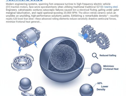
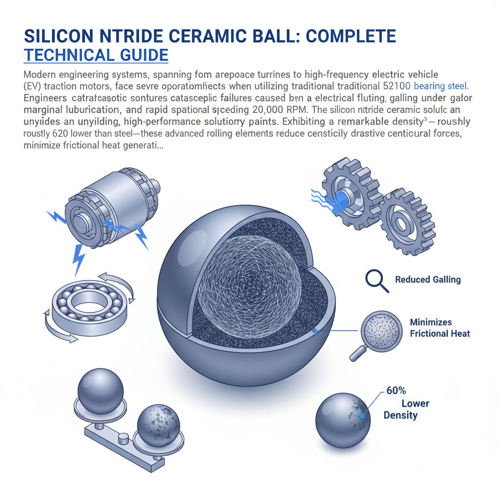
Zirconia Ceramic Ball for Semiconductor: Complete Technical Guide
As semiconductor manufacturing advances toward sub-3nm nodes, the demand for ultra-pure, defect-free components has never been higher. Contamination, mechanical wear. And chemical degradation in critical fluid handling and wafer processing equipment directly impact wafer yield. A ジルコニア ceramic ball for semiconductor applications presents an engineered solution to these pervasive industry pain points. By leveraging Yttria-Tetragonal Zirconia Polycrystal (Y-TZP), engineers can eliminate metallic particle generation, withstand aggressive planarization slurries. And operate seamlessly in ultra-high vacuum environments (10⁻⁸ Torr). This comprehensive technical guide explores the material physics, exact engineering specifications, comparative performance metrics. And rigorous manufacturing protocols required to produce semiconductor-grade zirconia spheres. Furthermore, we detail how Great Ceramic’s advanced capabilities achieve strict dimensional tolerances of ±0.005mm, ensuring frictionless operation and extended mean time between failures (MTBF) in next-generation fabrication equipment.
材料特性
Semiconductor-grade ジルコニア is predominantly formulated as 3 mol% Yttria-Stabilized Zirconia (3Y-TZP). The addition of yttrium oxide (Y₂O₃) stabilizes the tetragonal crystalline phase down to room temperature, a critical structural mechanism that prevents the destructive volumetric expansion (typically 3% to 5%) associated with the monoclinic transition. This precise stabilization matrix yields unparalleled fracture toughness, measuring between 8.0 and 10.0 MPa·m½. This effectively arrests micro-crack propagation when subjected to high-cycle mechanical stress in fab equipment.
Furthermore, this material exhibits an exceptional density of 6.05 g/cm³, providing immense structural rigidity and compressive strength exceeding 2,000 MPa. In semiconductor environments where dielectric isolation is mandatory, 3Y-TZP delivers an electrical resistivity greater than 10¹⁰ Ω·cm at 20°C, completely mitigating static discharge risks near sensitive IC architectures. With a virtually zero porosity matrix (less than 0.1% water absorption), outgassing in high-vacuum deposition chambers is eradicated.
| プロパティ | 価値 | 単位 |
|---|---|---|
| 密度 | 6.05 | g/cm³ |
| 硬度 | 1250 | HV |
| 曲げ強度 | 1050 | MPa |
| 破壊靭性 | 9.5 | MPa-m½ |
| 熱伝導率 | 2.2 | W/m-K |
| 電気抵抗率 | >10¹⁰ | Ω・cm |
| 最高使用温度 | 1000 | °C |
The specific heat capacity of this engineered ceramic remains stable at 400 J/kg·K. This combined with its notably low thermal conductivity (2.2 W/m·K), makes it an outstanding thermal insulator for hot-zone isolation in High-Temperature Chemical Vapor Deposition (HTCVD) systems. The coefficient of thermal expansion (CTE) registers at 10.5 × 10⁻⁶/°C (from 20 to 400°C), closely matching specific high-performance alloys to allow for precise interference fits in complex metallic assemblies.
他のセラミックとの比較
When selecting a bearing or valve component for wafer processing, engineers must evaluate a highly specialized matrix of tribological, thermal. And mechanical data. While アルミナ/アルミナ provides a cost-effective solution for less demanding environments, its lower fracture toughness (4.5 MPa·m½) limits its viability under the high-impact shock loads encountered in rapid wafer handling robotics. A zirconia ceramic ball for semiconductor applications excels precisely where alumina fails, offering more than double the fracture toughness and significantly superior wear resistance against nano-silica CMP slurries.
Conversely, 窒化ケイ素 provides a lower density profile (3.20 g/cm³) and superior high-temperature operational thresholds (up to 1200°C continuous), making it the primary choice for ultra-high-speed spindle bearings. However, Y-TZP zirconia offers a uniquely superior surface finish potential (capable of Ra 0.005µm) and unmatched chemical inertness in highly basic environments (pH > 12). This is paramount for specific liquid chemical delivery systems. Additionally, zirconia outperforms 炭化ケイ素 in shock absorption, as SiC’s extreme rigidity (Young’s Modulus of 410 GPa) makes it brittle under dynamic mechanical loads.
| プロパティ | Zirconia Ceramic Ball for Semiconductor | アルミナ | ジルコニア | 窒化ケイ素 |
|---|---|---|---|---|
| 熱伝導率 | 2.2 | 30.0 | 2.5 | 29.0 |
| 硬度 | 1250 | 1600 | 1200 | 1500 |
| 破壊靭性 | 9.5 | 4.5 | 8.0 | 6.5 |
| コスト | 高い | 低い | ミディアム | 非常に高い |
Optimize Your Semiconductor Equipment Performance: Do you need assistance selecting the exact ceramic material grade for your high-vacuum or corrosive fluid application? Contact our materials engineering team today for a comprehensive design consultation.
アプリケーション
- Chemical Mechanical Planarization (CMP) Slurry Control Valves: In advanced node CMP processes, slurries utilize highly abrasive nano-ceria or silica particles suspended in aggressive chemistries (pH ranges from 2.0 to 12.0). A zirconia ceramic ball for semiconductor valves acts as the primary fluid control check mechanism. Engineers select this material because its 1250 HV hardness prevents micro-abrasion from the slurry, ensuring zero particle shedding and maintaining leak rates below 1×10⁻⁶ atm·cc/sec over a lifecycle exceeding 5 million cycles.
- Wafer Processing Vacuum Bearings: Standard steel bearings suffer from severe galling and cold-welding in ultra-high vacuum (UHV) environments (10⁻⁸ Torr) found in PVD and ion implantation chambers. Zirconia balls operate entirely unlubricated, preventing hydrocarbon contamination. Their non-magnetic nature (magnetic permeability < 1.00001) ensures they do not distort the sensitive electromagnetic fields utilized to guide ion beams or plasma confinement arrays.
- Wet Bench Fluid Handling Pumps: Automated wet stations utilizing Piranha etch (H₂SO₄/H₂O₂ at 120°C) or RCA cleans require diaphragm and check pumps with absolute chemical resistance. Y-TZP zirconia check balls resist aggressive acidic and alkaline attacks, exhibiting a corrosion rate of less than 0.01 mm/year in 10% HF solutions. This prevents heavy metal leaching (such as Fe, Ni, or Cr) that would severely degrade carrier minority lifetime in silicon wafers.
- Lithography Equipment Metrology Spheres: Extreme Ultraviolet (EUV) lithography systems require highly calibrated spherical targets for multi-axis laser interferometry. Zirconia is chosen for its ability to be polished to a Grade 3 specification (sphericity < 0.08 µm, surface roughness Ra < 0.005 µm). Its high density (6.05 g/cm³) provides vibration damping properties, ensuring geometric stability even under micro-seismic disturbances within the fab environment.
- Plasma Etch Chamber Positioning Components: Reactive Ion Etching (RIE) utilizes aggressive halogen-based plasmas (such as CF₄, Cl₂, HBr). Zirconia balls are employed in the kinematic coupling mechanisms of wafer chucks due to their high plasma erosion resistance. They maintain their sub-micron geometric tolerances even after hundreds of hours of exposure to high-density plasma operating at 1,000 W RF power, where metallic components would rapidly vaporize.
製造工程
The fabrication of a zirconia ceramic ball for semiconductor integration dictates absolute control over every phase of production, from raw powder synthesis to final nano-polishing. The process begins with ultra-high purity Y-TZP powders featuring an average particle size (D50) of precisely 0.3 to 0.5 µm. Powder morphology is strictly controlled to ensure homogeneous green-body density. Any agglomeration or impurity at the ppm level will result in catastrophic failure or contamination in the final semiconductor application. Great Ceramic employs a stringent, multi-stage manufacturing architecture designed to guarantee the ±0.005mm tight-tolerance required by Tier 1 equipment manufacturers.
成形方法
- 冷間静水圧プレス(CIP): For larger spherical components (typically > 10.0 mm in diameter), the prepared zirconia powder is encapsulated in a flexible elastomer mold and submerged in a highly pressurized fluid vessel. Hydraulic pressures ranging from 200 to 300 MPa are applied uniformly across all 360 degrees. This hydrostatic forming method achieves an exceptional green density of roughly 60% theoretical maximum, eliminating internal voids and density gradients that would otherwise cause anisotropic shrinkage during sintering.
- Ceramic Injection Molding (CIM): For micro-spheres (ranging from 1.0 mm to 5.0 mm), powders are compounded with proprietary thermoplastic binders to create a specialized feedstock. This feedstock is injected into precision multi-cavity tungsten carbide molds at temperatures between 160°C and 200°C and pressures exceeding 100 MPa. CIM allows for rapid scale-up while maintaining net-shape geometric consistency, prior to advanced catalytic or thermal debinding processes.
焼結
The transition from a fragile green body to a fully densified structural ceramic occurs via precisely profiled solid-state sintering. The spherical preforms are loaded onto refractory setter plates and processed in high-purity atmospheric kilns. The thermal profile is engineered to ramp up at exactly 1°C to 2°C per minute to prevent thermal shock, culminating in a soak temperature between 1450°C and 1550°C for 2 to 4 hours. During this phase, the material undergoes a massive volumetric shrinkage of 20% to 25%. Accurate thermodynamic control is paramount to achieve a final theoretical density of >99.9%, effectively sealing all interconnected porosity and achieving the required 6.05 g/cm³ physical density.
最終加工
Achieving semiconductor-grade dimensional accuracy requires advanced 精密セラミック加工 and multi-axial lapping operations. Post-sintering, the blanks possess a rough tolerance of ±0.2 mm. They are loaded into specialized grooved cast iron lapping plates and rotated in a planetary motion under heavy continuous downward pressure (ranging from 10 to 50 N per sphere). Successive stages of diamond abrasive paste, stepping down from 15 µm to sub-micron 0.25 µm grit, slowly remove surface material. This prolonged, geometrically complex lapping process ensures roundness, achieving Grade 5 or even Grade 3 specifications (sphericity deviation less than 0.13 µm and 0.08 µm respectively). The final chemical-mechanical polishing (CMP) step guarantees an ultra-smooth, scratch-free surface (Ra < 0.01 µm), essential for frictionless rolling contact.
利点と限界
メリット
- Zero Particle Shedding: Thanks to the 1250 HV hardness and high cohesive strength of the Y-TZP microstructure, a zirconia ceramic ball for semiconductor applications experiences negligible abrasive wear. This ensures class 10 cleanroom compliance, avoiding the generation of nanoscale particulate contaminants that would otherwise result in catastrophic yield losses in sub-10nm logic and memory nodes.
- 変形強化: When a micro-crack begins to propagate through the material under high mechanical stress, the stress field induces a phase transformation in the immediate vicinity of the crack tip. The crystal structure shifts from tetragonal to monoclinic, accompanied by a 3-5% localized volume expansion. This expansion actively compresses the crack, halting its progression and yielding a fracture toughness (9.5 MPa·m½) unmatched by other advanced technical ceramics.
- Supreme Chemical Inertness: Zirconia does not react with the vast majority of highly aggressive chemicals utilized in modern fab processes. It demonstrates total immunity to hydrofluoric acid (HF), hydrochloric acid (HCl). And heated sulfuric acid mixtures. Consequently, it maintains strict dimensional stability and prevents heavy metal ionic leaching into critical process fluids.
- High-Vacuum Compatibility: By achieving over 99.9% theoretical density and zero open porosity, these ceramic spheres prevent trapped gases from outgassing when subjected to ultra-high vacuum (UHV) pressures below 10⁻⁸ Torr. This ensures deposition integrity in Physical Vapor Deposition (PVD) and Atomic Layer Deposition (ALD) chambers.
制限事項
- Hydrothermal Aging Vulnerability: Under prolonged exposure to high-temperature moisture or steam environments (specifically between 200°C and 300°C), Y-TZP can undergo Low-Temperature Degradation (LTD). This environmental condition triggers spontaneous surface phase transformation from tetragonal to monoclinic, resulting in micro-cracking and a subsequent decrease in mechanical strength.
- High Mass Inertia: With a density of 6.05 g/cm³, zirconia is significantly heavier than silicon nitride (3.20 g/cm³) and standard bearing steel (7.80 g/cm³). In ultra-high-speed centrifugal applications (exceeding 50,000 RPM), the resulting centrifugal forces create extreme kinetic loads on the outer bearing races. This can limit the maximum continuous operating speeds compared to lighter ceramic alternatives.
加工に関する考慮事項
Transforming sintered Y-TZP blanks into flawless bearing components for the semiconductor sector poses profound engineering challenges. The very characteristic that makes a zirconia ceramic ball for semiconductor use so durable—its high fracture toughness and transformation toughening—renders it exceptionally difficult to machine. Conventional abrasive cutting mechanics often induce excessive subsurface damage due to localized frictional heating (exceeding 800°C at the tool-ceramic interface) and the subsequent stress-induced tetragonal-to-monoclinic phase shifts.
To overcome this, Great Ceramic utilizes rigid, high-damping machine architectures coupled with resin-bonded polycrystalline diamond (PCD) tooling. Grinding kinematics must be strictly controlled. feed rates are kept exceptionally low (e.g., 0.05 to 0.1 mm/min). And spindle speeds are optimized to maintain constant surface speed while heavily flooding the contact zone with highly lubricious, water-based synthetic coolants at 15-20 Bar pressure. This rapid heat evacuation prevents thermal shock micro-fractures.
For high-precision spherical lapping, achieving the required ±0.005mm dimensional tolerance and a sphericity of < 0.13 µm requires proprietary multi-directional planetary kinematics. The lapping loads must be meticulously distributed across hundreds of spheres simultaneously to prevent localized pressure spikes. Additionally, post-machining metrology is critical. every production batch is subjected to rigorous optical interferometry and laser scanning to verify that surface roughness (Ra) strictly adheres to the < 0.01 µm specification, guaranteeing zero asperity contact in high-vacuum mechanical integration.
Require Tight-Tolerance Ceramic Components? Great Ceramicの高度なマシニングセンターは、公差±0.005mmの精密部品を日常的に提供しています。. 迅速なRFQのためにCAD図面を提出してください。.
FAQ
半導体用ジルコニアセラミックボールとは?
半導体用ジルコニアセラミックボールは、イットリア安定化ジルコニア(Y-TZP)から製造される超高精度の球状部品です。マイクロエレクトロニクス製造装置用に特別に設計されたこの球は、絶対的な化学的不活性、高い機械的靭性が要求される環境で使用されます。また、パーティクルの発生もありません。超高真空蒸着チャンバー(10-20⁸ Torr)から過酷な化学的機械的平坦化(CMP)流体ラインまで、さまざまな条件下で使用されるこの球体は、シリコンウェーハ上の金属や微粒子の汚染を防ぐため、厳しい寸法公差(多くの場合±0.005mm)と高い表面仕上げ(Ra < 0.01μm)で厳密に製造されています。.
半導体用ジルコニアセラミックボールの主な用途は何ですか?
これらのエンジニアード・スフェアは、工場内の重要なサブシステムに配備されている。主な用途としては、化学的機械的平坦化(CMP)スラリー分配ポンプの高サイクル逆止弁として機能し、ナノシリカの研磨性に耐えます。高真空ロボット・ウェハー・ハンドラーの無潤滑非磁性ベアリング・エレメントとして、アウトガスの発生や冷間溶接を防止します。さらに、腐食性の高い酸(HFやPiranhaなど)を注入するウェットベンチの流体ハンドリングシステムにも使用されています。また、多軸極端紫外線(EUV)露光計測システムにおいて、寸法的に安定し、振動を減衰させるキャリブレーションターゲットとして機能します。.
半導体用ジルコニアセラミックボールは、他のセラミックと比較してどうですか?
標準的なテクニカル・セラミックスと比較した場合、ジルコニアは独自の地位を占めています。ジルコニアは高純度アルミナの2倍以上の破壊靭性(9.5対4.5MPa・m½)を持ち、高速自動化サイクルにおける衝撃や機械的疲労に対する耐性が大幅に向上しています。窒化ケイ素は、スピンドル・ベアリングに低密度と高速性を提供する一方で、ジルコニアは優れた表面仕上げ特性と強アルカリ溶液(pH > 12)に対する耐薬品性を強化します。さらに、ジルコニアは耐衝撃性において炭化ケイ素を完全に凌駕しており、極端な弾性率の硬質材料に伴う脆性粉砕のリスクを回避しています。.
半導体用ジルコニアセラミックボールの利点は何ですか?
その決定的な利点は、「変態強化」メカニズムにある。これは、応力下でのマイクロクラックの伝播を止め、比類のない機械的耐久性(曲げ強度1050MPa)を与える。この耐久性により、パーティクルの脱落がゼロとなる。これは、3nm以下のロジック・ノードで高いウェーハ歩留まりを維持するために必須である。さらに、超高密度(6.05g/cm³)と0%の開気孔率により、高真空環境におけるアウトガスのリスクを排除します。絶対的な化学的不活性により、プロセス流体への重金属イオンの溶出がありません。また、高い電気抵抗率(>10¹⁰ Ω-cm)により、繊細なマイクロ回路を容易に破壊する静電気の蓄積と放電を防ぎます。.
半導体用ジルコニアセラミックボールはどのように加工されるのですか?
焼結ジルコニアは、その極めて高い硬度と靭性により、加工が難しいことで知られています。Great Ceramicでは、±0.005mmの厳格な公差と0.13μm未満の真球度を達成するには、独自の多軸精密ラッピングが必要です。溝付き鋳鉄板またはポリウレタン板を装備した高剛性遊星ラッピングマシンを使用し、ダイヤモンド砥粒スラリーを15 µmから0.25 µm砥粒まで段階的に降下させながら、正確な下向きの力(10~50 N)を加えます。接触部での応力による相変態を防ぐため、大量のクーラント流が義務付けられています。当社の高度な 精密セラミック加工 は、鏡面仕上げ(Ra < 0.01 µm)の完璧なグレード5またはグレード3仕様を保証します。.
半導体部品用のカスタムジルコニアセラミックボールが必要ですか? グレート・セラミックへのお問い合わせ 公差の厳しい精密機械加工サービスについては、Eメールでお問い合わせください。 [email protected].
半導体用ジルコニアセラミックボールは、先端セラミック用途に広く使用されています。.
詳細はこちら 半導体用ジルコニアセラミックボール および当社の精密セラミック加工サービス。.