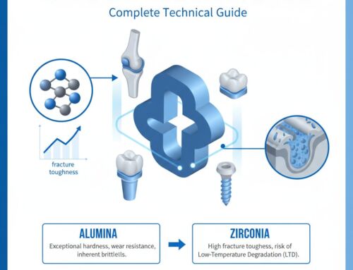
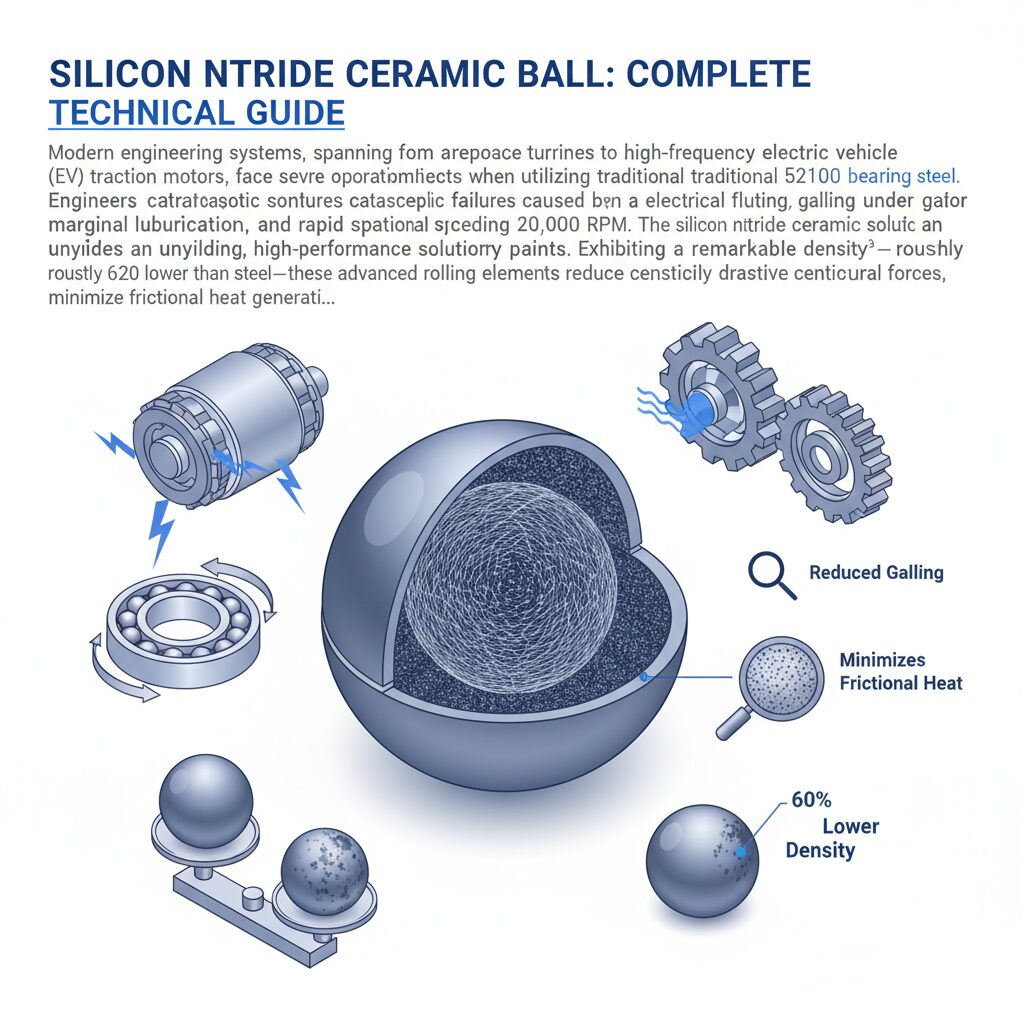
Silicon Carbide Ceramic Substrate for Energy: Complete Technical Guide
In the rapidly evolving renewable energy and high-power electronics sectors, thermal management remains a critical engineering bottleneck. A 炭化ケイ素 ceramic substrate for energy applications provides the ultimate thermal and electrical foundation for high-voltage, high-frequency systems. Operating at temperatures exceeding 1,000°C and handling extreme power densities that cause standard legacy materials to fail catastrophically, 炭化ケイ素 (SiC) drastically outperforms traditional substrates. It offers exceptional thermal conductivity (up to 170 W/m·K) combined with robust dielectric strength and mechanical rigidity. For engineers designing electric vehicle (EV) traction inverters, solar photovoltaics. And high-capacity wind turbine power modules, achieving optimal heat dissipation without compromising electrical insulation is a non-negotiable requirement.
This comprehensive technical guide deeply explores the physical properties, comparative advantages. And precision manufacturing requirements of SiC substrates. As system voltages in the energy sector push past 800V toward 1200V and beyond, the thermal load on semiconductor dies increases exponentially. Relying on standard substrates leads to thermal runaway and system failure. At Great Ceramic, we specialize in overcoming the innate brittleness and extreme hardness of these advanced materials, delivering 精密セラミック加工 with ultra-tight tolerances of ±0.005mm. Whether you are scaling up renewable grid infrastructure or developing next-generation energy storage components, understanding how to specify, deploy. And machine these advanced substrates is vital for project success and long-term reliability.
材料特性
The performance of a silicon carbide ceramic substrate for energy is dictated by its unique covalent bonding and crystalline structure. SiC exists in various polytypes, with alpha-SiC (hexagonal crystal structure) being the most common for high-performance sintered substrates. The incredibly strong silicon-to-carbon bonds result in a material that is exceptionally hard, thermally conductive. And chemically inert. In high-power energy applications, the ability to conduct heat away from active semiconductor junctions while maintaining electrical isolation is the primary metric of success. Below is a detailed breakdown of the standard thermomechanical and electrical properties of sintered silicon carbide.
| プロパティ | 価値 | 単位 |
|---|---|---|
| 密度 | 3.15 – 3.20 | g/cm³ |
| 硬度 | 2500 – 2800 | HV |
| 曲げ強度 | 400 – 450 | MPa |
| 破壊靭性 | 4.0 – 4.5 | MPa-m½ |
| 熱伝導率 | 120 – 170 | W/m-K |
| 電気抵抗率 | > 10^5 (Insulating Grades) | Ω・cm |
| 最高使用温度 | 1400 – 1650 | °C |
To fully grasp the engineering value of these metrics, one must look at their synergy. The thermal conductivity of 120-170 W/m·K is critical for rapidly dissipating heat fluxes that often exceed 300 W/cm² in modern insulated-gate bipolar transistor (IGBT) and SiC MOSFET modules. Furthermore, the maximum working temperature of up to 1650°C ensures that even under severe thermal shock conditions, the substrate will not melt, warp, or degrade. However, the extreme hardness (up to 2800 HV) presents significant challenges in shaping and finishing the material, requiring specialized diamond grinding techniques to achieve the precise flatness and surface finish necessary for direct bonded copper (DBC) or active metal brazing (AMB) processes.
他のセラミックとの比較
When selecting a substrate for energy applications, engineers must balance thermal conductivity, mechanical strength. And production costs. While a silicon carbide ceramic substrate for energy is a premium choice, it is essential to benchmark it against other widely utilized technical ceramics to justify its deployment in specific high-stress environments.
| プロパティ | 炭化ケイ素 | アルミナ | ジルコニア | 窒化ケイ素 |
|---|---|---|---|---|
| 熱伝導率 (W/m-K) | 120 – 170 | 24 – 35 | 2 – 3 | 30 – 90 |
| 硬度(HV) | 2500 – 2800 | 1500 – 1650 | 1200 - 1300 | 1500 – 1600 |
| 破壊靭性 (MPa-m½) | 4.0 – 4.5 | 3.5 – 4.0 | 8.0 - 10.0 | 6.5 – 8.0 |
| コスト | 高い | 低い | ミディアム | 高い |
Silicon Carbide vs. Alumina: アルミナ/”>Alumina (Al2O3) is the most ubiquitous ceramic substrate due to its low cost and adequate electrical insulation. However, its thermal conductivity peaks at roughly 35 W/m·K. In high-power energy systems, such as 800V EV inverters, alumina cannot dissipate heat fast enough, leading to thermal bottlenecks. Silicon carbide offers up to five times the thermal conductivity of alumina, making it vastly superior for high-power-density applications, despite the higher cost.
Silicon Carbide vs. Zirconia: ジルコニア (ZrO2) is renowned for its exceptional fracture toughness (up to 10.0 MPa·m½), making it highly resistant to impact and mechanical stress. However, as an energy substrate, it fails fundamentally due to its abysmal thermal conductivity (2-3 W/m·K), acting as a thermal insulator rather than a conductor. Zirconia is better suited for structural wear parts rather than thermal management in power electronics.
Silicon Carbide vs. Silicon Nitride: 窒化ケイ素 (Si3N4) is SiC’s primary competitor in the high-end power module market. Silicon nitride offers exceptional mechanical reliability and higher fracture toughness (up to 8.0 MPa·m½), making it highly resilient to the thermal cycling stresses associated with copper-clad substrates. However, standard silicon nitride has a thermal conductivity of 30-90 W/m·K. This falls short of silicon carbide’s 120-170 W/m·K. For absolute maximum heat dissipation, SiC remains the superior choice.
It is also worth noting that 窒化アルミニウム (AlN) is another high-thermal-conductivity option (up to 170-200 W/m·K), but SiC generally offers better mechanical hardness and chemical stability under extreme environmental conditions. Similarly, while 窒化ホウ素 offers excellent lubricity and thermal properties, it lacks the structural rigidity of a sintered SiC substrate.
アプリケーション
The deployment of a silicon carbide ceramic substrate for energy systems is rapidly expanding. As the global push for electrification and renewable energy intensifies, the demands placed on electronic control and power distribution modules have exceeded the capabilities of conventional materials. Below are the primary application domains where SiC substrates are fundamentally changing engineering parameters.
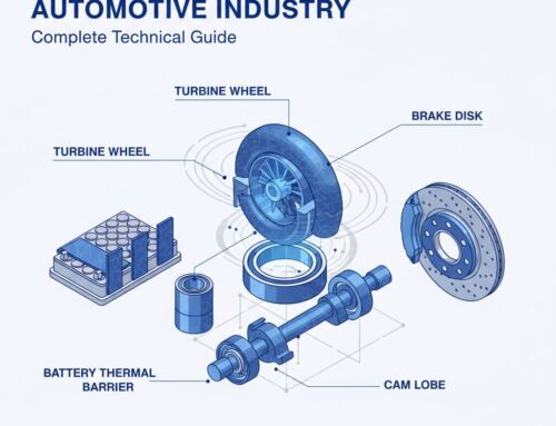
- Electric Vehicle (EV) Traction Inverters: In modern 800V and upcoming 1200V EV architectures, traction inverters convert DC battery power into AC power for the motors. The switching frequencies (often exceeding 100 kHz) generate massive heat fluxes. Silicon carbide substrates are utilized as the foundation for these power modules because their high thermal conductivity (150 W/m·K) quickly draws heat away from the semiconductor dies. Additionally, SiC’s coefficient of thermal expansion (CTE) of ~4.0 x 10^-6/K closely matches that of the silicon and SiC semiconductor chips, preventing solder layer fatigue and delamination during rapid acceleration and deceleration cycles.
- Solar Photovoltaic (PV) Inverter Modules: Utility-scale solar farms require high-efficiency string and central inverters to minimize power conversion losses. These systems operate outdoors, enduring extreme ambient temperature fluctuations and high UV exposure. SiC substrates are chosen for PV inverters because they allow the power modules to operate at higher junction temperatures (up to 175°C – 200°C) without degradation. This reduces the need for massive, heavy aluminum heat sinks or liquid cooling loops, thereby increasing the overall volumetric power density of the solar inverter system.
- Wind Turbine Power Converters: Offshore wind turbines, generating upwards of 12-15 MW per unit, rely on massive power conversion systems situated in the nacelle. Maintenance in these environments is prohibitively expensive. SiC ceramic substrates are selected for the IGBT and MOSFET modules in these converters because of their unparalleled long-term reliability. The chemical inertness of SiC protects the substrate from high-humidity, salt-fog environments, while its mechanical rigidity prevents micro-cracking caused by constant low-frequency vibrational stress from the turbine blades.
- High-Voltage Direct Current (HVDC) Transmission Systems: Moving renewable energy from remote generation sites (like offshore wind or desert solar) to urban centers requires HVDC lines operating at hundreds of kilovolts. The thyristor valves and conversion stations rely on semiconductor networks that handle massive current loads. SiC substrates provide the extreme dielectric strength (up to 30 kV/mm) necessary to prevent electrical arcing and short circuits in these multi-megawatt stations, while simultaneously providing a thermal highway to dissipate the inherent conversion losses.
- Nuclear Reactor Sensor Housings and Control Substrates: Advanced small modular reactors (SMRs) and generation-IV nuclear systems operate at temperatures that melt standard electronics. Furthermore, these environments are subjected to high levels of neutron radiation. SiC substrates are chosen because silicon carbide exhibits exceptional radiation hardness. Unlike polymers or standard glasses that degrade and become brittle under neutron bombardment, the rigid crystalline lattice of SiC maintains its structural and thermal integrity, ensuring that critical temperature and pressure monitoring sensors continue to function safely over decades of operation.
製造工程
Transforming raw silicon carbide powder into a highly precise silicon carbide ceramic substrate for energy applications is a complex, multi-stage metallurgical and ceramic engineering process. Achieving the exact stoichiometric balance, density. And dimensional accuracy requires strict environmental controls and advanced machinery. The process is broadly categorized into forming, sintering. And final precision machining.
成形方法
- Tape Casting: This is the dominant method for producing thin, flat ceramic substrates. Sub-micron silicon carbide powder is mixed with specific organic binders, plasticizers. And dispersants to create a viscous slurry. This slurry is precisely cast onto a moving carrier film using a doctor blade assembly. The gap of the doctor blade dictates the unfired (green) thickness. This typically ranges from 0.3mm to 1.5mm. After drying, the green tape is highly uniform and can be laser-cut or punched into specific substrate geometries before firing.
- Isostatic Pressing: For thicker substrates or complex 3D heat sink geometries, cold isostatic pressing (CIP) is utilized. The SiC powder is enclosed in a flexible elastomer mold and subjected to uniform fluid pressure (often exceeding 200 MPa) from all directions. This creates a high-density green body with minimal density gradients. This is crucial for preventing warpage during the high-temperature sintering phase.
焼結
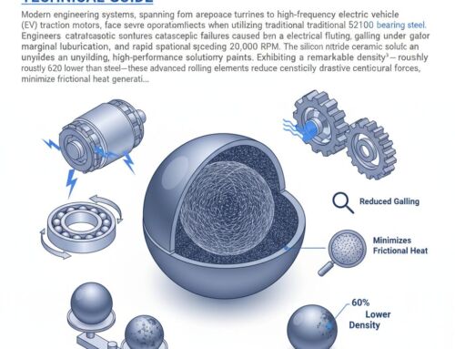
The sintering of silicon carbide is notoriously difficult due to the strong covalent bonds. This inhibit atomic diffusion at normal sintering temperatures. To achieve near-theoretical density (>98%), the green bodies undergo pressureless sintering in a vacuum or inert argon atmosphere at extreme temperatures ranging from 2100°C to 2200°C. Sintering aids, such as boron and carbon, are often added in fractional percentages to facilitate densification. During this phase, the organic binders burn off completely. And the material undergoes a volumetric shrinkage of 15% to 20%. Controlling the thermal gradient during the cooling phase is absolutely critical to prevent residual internal stresses that could lead to spontaneous micro-cracking of the substrate.
最終加工
Because the sintered silicon carbide substrate is exceptionally hard (up to 2800 HV), conventional cutting tools are useless. Final machining requires advanced super-abrasive technology. The substrates undergo double-sided lapping using boron carbide or diamond slurries to achieve strict flatness and parallelism specifications (often < 2 µm). This is followed by chemical-mechanical polishing (CMP) to achieve a mirror-like surface roughness of Ra < 0.05 µm. This flawless surface is an absolute prerequisite for the subsequent metallization processes (like AMB or DBC) required to bond copper circuits to the ceramic.
Optimize your supply chain with advanced technical ceramics. グレート・セラミックへのお問い合わせ today to discuss how our custom forming and sintering capabilities can meet your exact energy project specifications.
利点と限界
While a silicon carbide ceramic substrate for energy is a highly advanced engineering solution, it is vital to understand both its transformative benefits and its inherent material constraints to ensure proper application design.
メリット
- Exceptional Thermal Conductivity: At 120-170 W/m·K, SiC vastly outperforms standard alumina substrates. This allows for rapid heat extraction from high-power density chips, lowering the junction temperature, extending the lifespan of the semiconductor. And improving the overall efficiency of the energy conversion module.
- Matched Coefficient of Thermal Expansion (CTE): The CTE of SiC (~4.0 x 10^-6/K) is remarkably close to that of the silicon (Si) and silicon carbide (SiC) semiconductor chips mounted on it. This precise matching minimizes the thermo-mechanical shear stress placed on the solder joints during rapid power cycling, effectively eliminating a primary failure mode in EV and solar inverters.
- High Breakdown Voltage: Energy systems operate at lethal voltages. SiC substrates possess high dielectric strength, ensuring complete electrical isolation between the high-voltage circuitry and the liquid cooling plates or grounded chassis, even when the substrate is manufactured at thicknesses of less than 1.0mm.
- 極度の化学的不活性: SiC is highly resistant to oxidation, acidic. And alkaline corrosion. In harsh operational environments, such as geothermal energy extraction or offshore wind deployments, the substrate will not degrade, oxidize, or lose its structural integrity over a decades-long lifespan.
制限事項
- High Machining and Manufacturing Costs: The extreme hardness of SiC means that shaping, grinding. And polishing the material requires expensive diamond tooling and significantly longer machine cycle times compared to alumina. The high-temperature (2100°C) sintering process also consumes vast amounts of energy, making the final substrate relatively expensive.
- Inherent Brittleness and Low Fracture Toughness: With a fracture toughness of ~4.0 to 4.5 MPa·m½, SiC is a brittle ceramic. It is susceptible to chipping or catastrophic fracture if subjected to sharp mechanical impacts, point loads, or improper handling during the assembly and torque-down phases of power module manufacturing.
加工に関する考慮事項
The greatest barrier to deploying a silicon carbide ceramic substrate for energy applications is the extreme difficulty of final stage machining. SiC’s hardness (second only to diamond and boron carbide) causes rapid tool wear, while its low fracture toughness makes it highly prone to edge chipping and subsurface micro-cracking during material removal. Conventional CNC machining parameters will instantly destroy both the tool and the workpiece.
To successfully machine SiC substrates, engineers must utilize ductile-regime grinding. By keeping the depth of cut extremely shallow (often less than 1 micrometer per pass) and utilizing ultra-fine diamond grinding wheels (e.g., D46 to D15 grit sizes), the SiC material can be removed through plastic deformation rather than brittle fracture. This minimizes subsurface damage and ensures structural integrity. Furthermore, high-pressure, specifically formulated aqueous coolants must be directed precisely at the cutting zone to flush away abrasive swarf and prevent thermal damage to the diamond matrix.
At Great Ceramic, we have mastered the art of precision hard-brittle material processing. Our state-of-the-art multi-axis CNC grinding centers, coupled with proprietary diamond tooling strategies, allow us to machine complex SiC substrate features—including through-holes, stepped edges. And custom cooling fins—with ultra-tight tolerances of ±0.005mm. We routinely achieve surface flatness of < 2 µm and roughness of Ra < 0.05 µm, ensuring your substrates are perfectly prepared for metallization and die bonding without the risk of hot-spots caused by microscopic air gaps.
FAQ
What is a silicon carbide ceramic substrate for energy?
A silicon carbide ceramic substrate for energy is a high-performance, flat insulating base used primarily in high-power electronics and renewable energy systems. Manufactured from sintered silicon carbide powder, it serves as the foundational layer upon which semiconductor chips (like IGBTs or SiC MOSFETs) are mounted. Its primary function is to provide absolute electrical isolation between the live circuits and the cooling system while simultaneously acting as a highly efficient thermal bridge to draw intense heat away from the active electronic components, preventing thermal failure in energy systems.
What are the main applications of a silicon carbide ceramic substrate for energy?
These substrates are heavily utilized in applications characterized by high voltages, high frequencies. And extreme thermal loads. The primary applications include electric vehicle (EV) traction inverters, where they handle the heat generated by converting DC battery power to AC motor power. They are also central to solar photovoltaic (PV) central inverters, wind turbine offshore power converters, high-voltage direct current (HVDC) grid transmission infrastructure. And specialized high-temperature sensors in advanced nuclear reactor cores.
How does a silicon carbide ceramic substrate compare to other ceramics?
Compared to standard alumina, a silicon carbide substrate offers up to five times the thermal conductivity (150 W/m·K vs 30 W/m·K), making it vastly superior for heat dissipation, though it is more expensive. Compared to zirconia, SiC is much harder and significantly more thermally conductive, whereas zirconia is essentially a thermal insulator. Compared to silicon nitride, SiC offers better thermal conductivity but slightly lower fracture toughness. Therefore, SiC is chosen when absolute maximum heat transfer and CTE matching with silicon dies are the top engineering priorities.
What are the advantages of using a silicon carbide ceramic substrate for energy?
The primary advantages include unparalleled thermal conductivity (up to 170 W/m·K). This allows power modules to operate at higher power densities and reduced sizes. It features a Coefficient of Thermal Expansion (CTE) that closely mimics the semiconductor chips it supports, drastically reducing thermo-mechanical stress and extending the module’s fatigue life. Additionally, SiC offers exceptional dielectric breakdown strength for high-voltage isolation, superior chemical resistance against harsh environmental factors. And the ability to maintain structural integrity at operating temperatures exceeding 1,000°C.
How is a silicon carbide ceramic substrate machined?
Machining SiC is exceptionally challenging due to its hardness (up to 2800 HV) and brittleness. It cannot be machined using standard high-speed steel or carbide tools. Instead, it requires specialized precision CNC grinding utilizing custom-profiled diamond grinding wheels. The process involves ductile-regime grinding with microscopic depths of cut and heavy flood coolant to prevent thermal damage and edge chipping. At Great Ceramic, our advanced 精密セラミック加工 capabilities allow us to process these highly resilient substrates to ultra-tight tolerances of ±0.005mm, achieving the pristine flatness and surface finishes required for advanced energy applications.
Need custom silicon carbide ceramic substrate for energy parts? グレート・セラミックへのお問い合わせ 公差の厳しい精密機械加工サービスについては、Eメールでお問い合わせください。 [email protected].
silicon carbide ceramic substrate for energy is widely used in advanced ceramic applications.
詳細はこちら Silicon Carbide Ceramic Substrate For Energy および当社の精密セラミック加工サービス。.