Machinable Glass Ceramic Ceramic Block for Semiconductor: Complete Technical Guide
In modern microelectronics manufacturing, selecting the optimal insulating material is critical to minimizing particulate contamination and maximizing wafer yield. The integration of a machinable glass ceramic ceramic block for semiconductor applications resolves a primary industry pain point: the high cost and 10-14 week lead times associated with diamond-grinding traditional technical ceramics. With a highly unique microstructure composed of 55% fluorophlogopite mica crystals embedded within a 45% borosilicate glass matrix, this advanced material allows for rapid, ultra-precise CNC machining using conventional carbide tooling. Great Ceramic specializes in transforming these raw machinable ceramic blocks into complex, tight-tolerance (±0.005mm) components tailored for high-vacuum, high-voltage. And corrosive plasma environments. Capable of withstanding continuous temperatures up to 800°C and boasting a zero-porosity structure that eliminates outgassing, it is the premier choice for rapid R&D prototyping and high-mix, low-volume semiconductor fabrication. Submit your RFQ to Great Ceramic today for custom components engineered to exact semiconductor specifications.
Materialeigenschaften
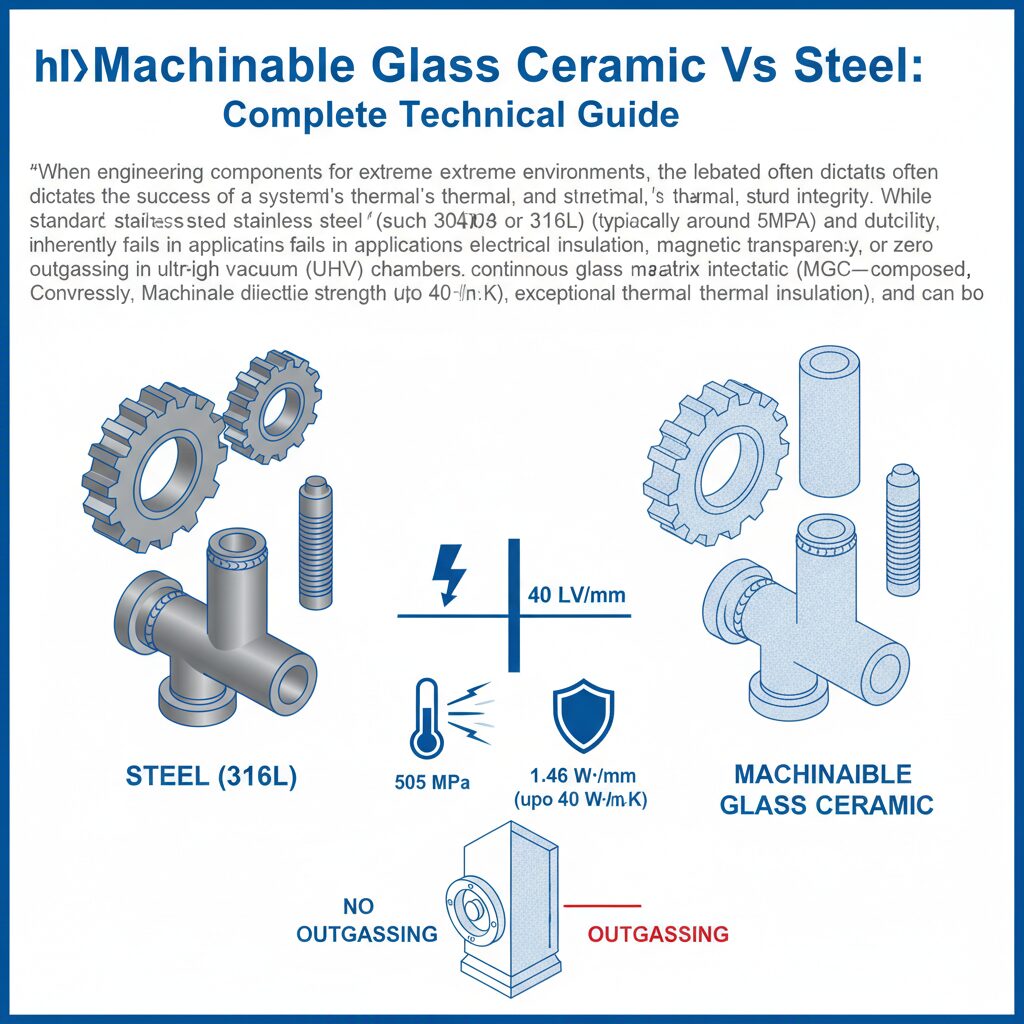
The technical efficacy of a machinable glass ceramic ceramic block for semiconductor applications originates from its highly engineered physical, thermal. And electrical properties. By controlling the crystallization process, the material achieves a density of 2.52 g/cm³, ensuring lightweight yet rigid structural support for 300mm wafer handling equipment. The 0% porosity characteristic translates to an operational vacuum compatibility of up to 10^-10 Torr, completely eradicating the moisture absorption (0.00% water absorption rate) that plagues conventional porous insulators.
Electrically, the borosilicate matrix provides an exceptional dielectric strength of 40 kV/mm at 25°C, functioning as an impenetrable barrier against electron tunneling during high-voltage ion implantation. Thermally, the coefficient of thermal expansion (CTE) is calculated at 9.3 × 10^-6 /°C (from 20°C to 300°C), matching several critical metals used in semiconductor assemblies. This reduces interfacial stress by up to 65% during thermal cycling. Below is the comprehensive data profile of the material.
| Eigentum | Wert | Einheit |
|---|---|---|
| Dichte | 2.52 | g/cm³ |
| Härte | 250 | HV |
| Biegefestigkeit | 94 | MPa |
| Bruchzähigkeit | 1.53 | MPa-m½ |
| Wärmeleitfähigkeit | 1.46 | W/m-K |
| Elektrischer spezifischer Widerstand | > 10^16 | Ω-cm |
| Maximale Betriebstemperatur | 800 | °C |
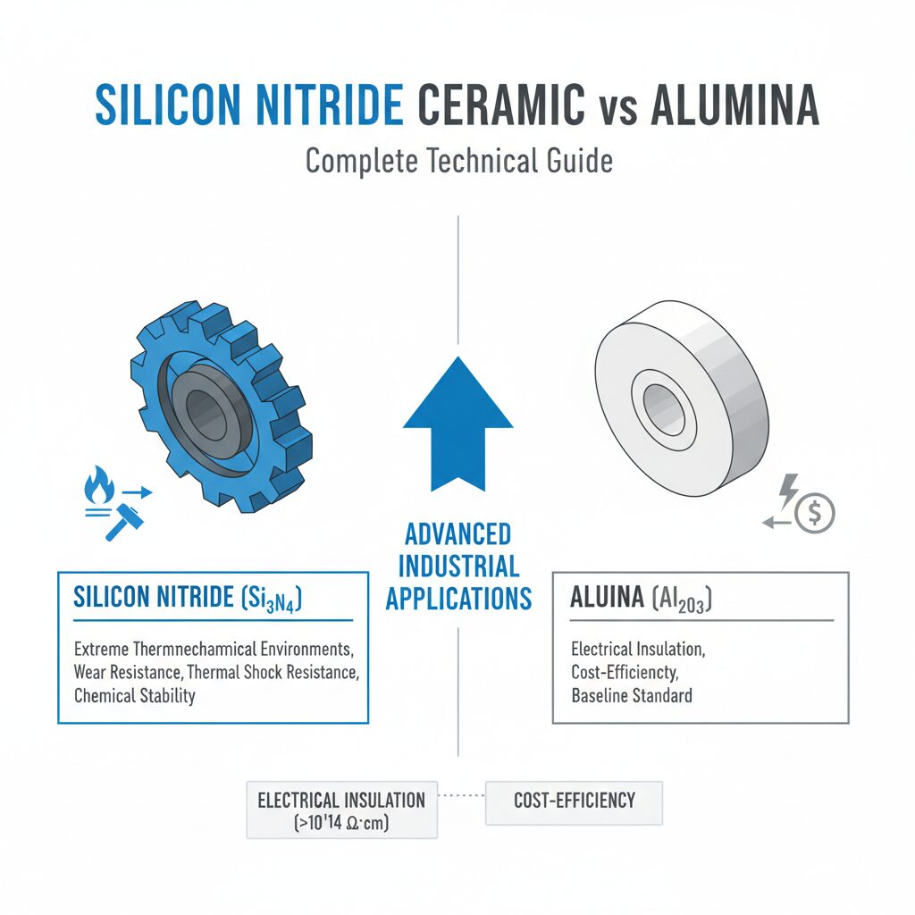
Vergleich mit anderen Keramiken
When engineering semiconductor capital equipment, procurement managers must evaluate trade-offs between machinability, thermal conductivity. And mechanical strength. While a machinable glass ceramic ceramic block for semiconductor applications offers an unprecedented reduction in machining time—often reducing 40 hours of diamond grinding to just 4 hours of standard CNC milling—it exhibits different mechanical thresholds compared to standard sintered oxides or nitrides.
For example, Tonerde/”>Aluminiumoxid boasts a much higher flexural strength of 350 MPa and a thermal conductivity of 30 W/m·K, but requires specialized diamond tooling that increases prototype iteration costs by over 300%. Zirkoniumdioxid provides unmatched fracture toughness at 8.0 MPa·m½, but its high density of 6.0 g/cm³ can introduce excessive mass in rapid-actuation robotic arms. In high-temperature thermal management scenarios where over 150 W/m·K is required, materials like Aluminiumnitrid are superior, but they cannot be easily modified in situ. Finally, Siliziumnitrid offers a formidable 800 MPa flexural strength and excellent thermal shock resistance, but at a premium cost 4 to 5 times higher than machinable alternatives.
| Eigentum | Bearbeitbare Glaskeramik | Tonerde (99,5%) | Zirkoniumdioxid (Y-TZP) | Siliziumnitrid |
|---|---|---|---|---|
| Wärmeleitfähigkeit | 1,46 W/m-K | 30 W/m·K | 2,5 W/m·K | 30-90 W/m·K |
| Härte | 250 HV | 1500 HV | 1200 HV | 1500 HV |
| Bruchzähigkeit | 1,53 MPa-m½ | 4.0 MPa·m½ | 8,0 MPa·m½ | 6.5 MPa·m½ |
| Cost for Complex Machining | Niedrig | Hoch | Hoch | Sehr hoch |
Anwendungen
The unique intersection of high dielectric strength, zero outgassing. And sub-micron dimensional stability positions the machinable glass ceramic ceramic block for semiconductor use at the forefront of wafer fabrication technology. By isolating reactive plasmas and maintaining thermal boundaries, this material directly contributes to reducing defect rates in node sizes below 5nm. Common applications engineered by Great Ceramic include:
- Wafer Chucks and Susceptors: Utilized in lithography and inspection modules, the material is lapped to a flatness of <0.002mm. The low thermal conductivity (1.46 W/m·K) ensures that localized heating zones do not transfer thermal gradients across the 300mm wafer surface, preventing thermal warping.
- Plasma Etch Chamber Components: Selected for its high resistance to fluorinated and chlorinated plasma chemistries. The 0% porosity prevents the trapping of process gases. This reduces pump-down times by 25% and eliminates particle generation during 400-hour continuous etching cycles.
- Ion Implantation Insulators: Deployed in high-energy implanters where voltages exceed 200 kV. The material’s dielectric strength (40 kV/mm) and surface resistivity (>10^16 Ω·cm at 25°C) prevent catastrophic arcing and power losses in the accelerator column.
- Ultra-High Vacuum (UHV) Feedthroughs: Chosen for critical sensor isolation where the system must maintain a vacuum level of 10^-10 Torr. The absence of interconnected pores ensures a helium leak rate of less than 10^-10 atm cc/sec, preserving the integrity of chemical vapor deposition (CVD) environments.
- PVD Shadow Masks and Fixtures: Integrated into physical vapor deposition tools due to its ability to survive rapid thermal shocks from 20°C up to peak temperatures of 1000°C. The material maintains a tight tolerance of ±0.005mm without warping, ensuring sharp deposition boundaries on microchip substrates.
Herstellungsprozess
The production of a machinable glass ceramic ceramic block for semiconductor manufacturing is a highly controlled sequence of melting, forming. And specialized crystallization. Unlike traditional technical ceramics that undergo cold isostatic pressing and high-temperature sintering with 15-20% shrinkage, this material is cast as a glass and subsequently “cerammed” with zero shrinkage. This distinctive phase transformation is what locks in the precise ±0.000mm volumetric stability prior to final machining.
Formgebungsmethoden
- Glass Melting and Casting: Raw materials, including high-purity silica (SiO2), magnesium oxide (MgO), aluminum oxide (Al2O3). And potassium fluorosilicate (K2SiF6), are homogeneously melted in a platinum crucible at temperatures exceeding 1400°C. The molten glass is then continuously cast into large slabs or extruded into continuous rods up to 300mm in diameter.
- Annealing: The cast blocks are immediately transferred to an annealing lehr, cooling slowly from 600°C to 20°C over a 72-hour period. This critical step relieves internal residual stresses, reducing the optical birefringence to less than 10 nm/cm and preventing catastrophic fracturing during subsequent heating.
Sintering (Ceramming Process)
Instead of traditional sintering, the blocks undergo a highly precise two-stage thermal treatment known as ceramming. The glass is heated to approximately 800°C, inducing the nucleation of chondrodite crystals. The temperature is then elevated to roughly 950°C – 1000°C, where these nucleated sites grow into randomly oriented, interlocking 2-dimensional fluorophlogopite mica crystals (KMg3AlSi3O10F2). This process continues until the material consists of precisely 55% crystalline mica and 45% residual borosilicate glass. The random orientation of these highly flexible 5-10 micron crystals acts to deflect and arrest microscopic cracks, rendering the final block machinable.
Endbearbeitung
The cerammed blocks are dimensionally stabilized and ready for subtractive manufacturing. Due to the mica cleavage planes, standard high-speed steel (HSS) or tungsten carbide cutting tools can locally fracture the crystals at a microscopic scale, safely removing material without propagating bulk cracks. This process eliminates the need for expensive diamond grinding wheels and drastically cuts production time. To understand our comprehensive capabilities in this area, explore Great Ceramic’s Präzisionskeramikbearbeitung services.
Vorteile und Beschränkungen
Vorteile
- Rapid Prototyping Speed: The ability to utilize standard multi-axis CNC machines reduces component lead times from an average of 12 weeks to just 2-3 weeks, yielding a 75% increase in R&D iteration cycles.
- Zero Outgassing and Porosity: Achieving 0.00% water absorption and possessing no open micro-pores ensures rapid vacuum pump-downs to 10^-10 Torr, eliminating chamber contamination in critical CVD processes.
- High Dimensional Stability: Demonstrating zero post-machining shrinkage and a uniform CTE of 9.3 × 10^-6 /°C, the material maintains strict ±0.005mm tolerances even under continuous 800°C thermal loads.
- Superior Electrical Insulation: Offering an electrical resistivity of >10^16 Ω·cm and a dielectric constant of 6.03 at 1 MHz, it provides absolute isolation for highly sensitive RF and plasma-generating circuitry.
Beschränkungen
- Lower Mechanical Strength: With a flexural strength of 94 MPa, it cannot bear heavy mechanical impact or continuous high-stress dynamic loads, unlike Siliziumkarbid. This boasts a superior strength exceeding 400 MPa.
- Chemical Sensitivity to Strong Alkalis: While highly resistant to most acids, prolonged exposure to concentrated alkaline solutions (pH > 10) at temperatures above 150°C can degrade the borosilicate glass matrix, necessitating careful environmental control.
Überlegungen zur Bearbeitung
Transforming a raw machinable glass ceramic ceramic block for semiconductor applications into a high-precision component requires a deep understanding of its unique fracture mechanics. Although it is machinable, improper tooling or aggressive feed rates will result in edge chipping, surface micro-cracking. And compromised vacuum integrity. Great Ceramic leverages decades of B2B industrial expertise to overcome these specific machining challenges, ensuring optimal yields and a strict adherence to ±0.005mm tolerances.
The primary challenge lies in managing localized thermal buildup and tool deflection. Because the material has a low thermal conductivity of 1.46 W/m·K, heat generated during the cutting process does not dissipate into the ceramic. instead, it transfers into the cutting tool, causing rapid degradation of the cutting edge. To combat this, Great Ceramic utilizes C2-grade tungsten carbide tools and maintains a continuous flood of water-soluble coolant (specifically formulated to avoid chemical interaction with the glass matrix).
To achieve flawless surface finishes (Ra < 0.8 µm), strict cutting parameters must be observed. Below is our standard engineering data for machining this material:
| Bearbeitungsverfahren | Spindeldrehzahl (U/min) | Feed Rate (mm/rev) | Schnitttiefe (mm) |
|---|---|---|---|
| Drehen (Schruppen) | 400 – 600 | 0.10 – 0.20 | 2.00 – 4.00 |
| Turning (Finishing) | 800 – 1000 | 0.02 – 0.05 | 0.20 – 0.50 |
| Milling (End Mill) | 1000 – 1500 | 0.03 – 0.05 | 1.00 – 2.50 |
| Drilling (Peck Cycle) | 300 – 500 | 0.02 – 0.04 | Peck every 1.5mm |
Furthermore, breakout and edge chipping during drilling operations are mitigated by employing a backing plate of sacrificial material and utilizing a 118-degree drill point angle. Threading presents another specific challenge. to achieve precise M2 to M10 threads, Great Ceramic utilizes specialized single-point threading tools rather than standard taps, ensuring the interlocking mica crystals shear cleanly without inducing localized hoop stress. To leverage our expertise in manufacturing highly complex geometries without scrap waste, contact the engineering team at Great Ceramic.
FAQ
What is a machinable glass ceramic ceramic block for semiconductor?
It is an advanced technical material composed of 55% fluorophlogopite mica crystals dispersed throughout a 45% borosilicate glass matrix. This highly engineered microstructure allows the block to be machined using standard CNC metalworking tools to extremely tight tolerances (±0.005mm). It is heavily utilized in the semiconductor industry because it offers zero porosity, requires no post-machining firing (0% shrinkage). And maintains structural and electrical integrity in vacuum environments up to 800°C.
What are the main applications of a machinable glass ceramic ceramic block for semiconductor?
The primary applications revolve around high-vacuum, high-voltage. And cleanroom environments in wafer fabrication. Specific uses include precision wafer chucks, susceptors, PVD/CVD thermal insulators, RF windows, high-voltage feedthroughs for ion implanters. And plasma etch chamber liners. The material is chosen for these components because its 1.46 W/m·K thermal conductivity and lack of outgassing help maximize chip yield and maintain stable cleanroom conditions.
How does a machinable glass ceramic compare to other ceramics?
Unlike sintered oxides or nitrides that require costly and time-consuming diamond grinding, machinable glass ceramics dramatically reduce fabrication time. While it has a lower flexural strength (94 MPa) compared to structural materials like Siliziumnitrid (800 MPa), its ability to be rapidly shaped makes it unparalleled for complex prototyping. Additionally, for ultra-high temperature applications requiring superior thermal shock resistance and lubrication, materials like Bornitrid may be utilized, but machinable glass ceramic remains the standard for rigid, zero-porosity vacuum insulation.
What are the advantages of using this machinable block?
The definitive advantage is the radical acceleration of manufacturing timelines, allowing engineers to receive complex parts in weeks rather than months. Technically, its advantages include a 0.00% water absorption rate, continuous operation at 800°C (with peak survivability up to 1000°C), an exceptional dielectric strength of 40 kV/mm. And a CTE of 9.3 × 10^-6 /°C that closely matches metals like stainless steel and titanium, thereby minimizing thermal stress in hybrid assemblies.
How is a machinable glass ceramic ceramic block for semiconductor machined?
It is machined subtractively via highly controlled CNC milling, turning. And drilling using C2-grade carbide tooling. Because the material fractures microscopically along the cleavage planes of the mica crystals, precise spindle speeds (1000-1500 RPM for milling) and exceptionally light feed rates (0.02-0.05 mm/rev) must be employed. Constant water-soluble coolant is required to prevent thermal degradation of the tooling. Great Ceramic excels in this specific process, consistently delivering complex geometries with surface finishes below 0.8 µm and dimensional tolerances tighter than ±0.005mm without inducing micro-fractures.
Need custom machinable glass ceramic ceramic block for semiconductor parts? Kontakt zu Great Ceramic für Präzisionsbearbeitungsleistungen mit engen Toleranzen oder per E-Mail [email protected] to discuss your specific engineering requirements and receive a rapid RFQ response.
machinable glass ceramic ceramic block for semiconductor is widely used in advanced ceramic applications.
Erfahren Sie mehr über Machinable Glass Ceramic Ceramic Block For Semiconductor und unsere Dienstleistungen im Bereich der keramischen Präzisionsbearbeitung.