Применение передовой керамики в полупроводниковой и электронной промышленности

Индустрия полупроводников и электронных компонентов требует материалов, которые могут надежно работать в экстремальных условиях - при высоких температурах, быстрой термоциклической обработке, высоком напряжении и сверхчистых производственных средах. Усовершенствованная керамика стали незаменимы в этой области благодаря исключительному сочетанию механической прочности, электроизоляции, термостойкости и химической инертности. Такие материалы, как глинозем (Al₂O₃), нитрид алюминия (AlN), нитрид кремния (Si₃N₄), диоксид циркония (ZrO₂), оксид бериллия (BeO), и нитрид бора (BN) широко используются в оборудовании для обработки полупроводников, микроэлектронной упаковке и высокопроизводительных электронных устройствах.
Ключевые преимущества передовой керамики для полупроводников и электроники
выгода:
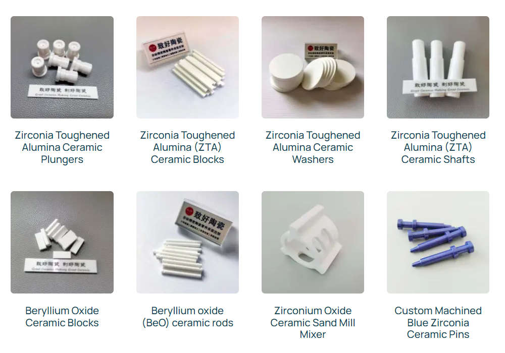
Ключевые материалы для применения в полупроводниках и электронике
Компания Great Ceramic стремится к расширению применения высокоэффективной керамики в полупроводниковой и электронной промышленности, помогая нашим клиентам достичь беспрецедентных уровней производительности, надежности и экологичности.
| Материал | Основные свойства | Типовые применения |
|---|---|---|
| Глинозем (Al₂O₃) | Экономичность, хорошая изоляция, умеренная теплопроводность | Подложки для светодиодов, многослойные упаковки, керамические печатные платы |
| Нитрид алюминия (AlN) | Высокая теплопроводность, электроизоляция, соответствие CTE с Si | Подложки для силовых модулей, теплораспределители для радиочастотных устройств |
| Нитрид кремния (Si₃N₄) | Высокая вязкость разрушения, устойчивость к термическим ударам | Руки для обработки пластин, подложки для силовой электроники |
| Карбид кремния (SiC) | Высокая прочность, коррозионная стойкость, термостойкость | Компоненты CVD-камер, футеровка диффузионных печей |
| Нитрид бора (BN) | Теплопроводник + электроизолятор, поддается обработке | Теплоотводы для радиочастотных/микроволновых устройств, интерфейсные слои |
| Стеклокерамика, поддающаяся механической обработке (MGC) | Легкая точная обработка, стабильность до 1000°C | Прототипирование деталей, мелкосерийные прецизионные компоненты |
| ZTA (циркониевый упрочненный глинозем) | Высокая износостойкость, повышенная вязкость разрушения | Прецизионные направляющие, инструменты для обработки полупроводников |
Эксплуатационные преимущества перед металлами и пластиками
| Недвижимость | Передовая керамика | Металлы | Пластмассы |
|---|---|---|---|
| Теплопроводность | Высокая (AlN до 260 Вт/м-К) | Умеренный (Cu: ~400 Вт/м-К) | Низкий (<1 Вт/м-К) |
| Электрическая изоляция | Отлично (>10¹³ Ω-см) | Бедный | Хорошо |
| Устойчивость к коррозии | Превосходно | Умеренно/Неудовлетворительно | Хорошо |
| Высокотемпературная стабильность | Превосходно (>1000°C) | Хорошо (500-800°C) | Плохое (<200°C) |
| Износостойкость | Превосходно | Хорошо | Бедный |
Ключевые приложения
Возможности производства керамики полупроводникового класса
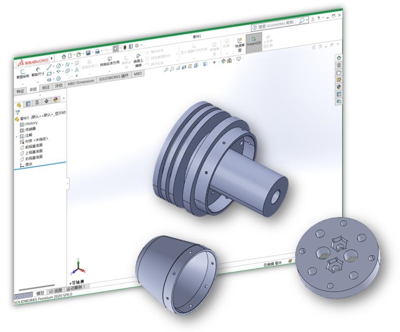
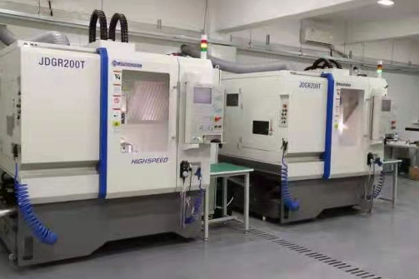
В компании Great Ceramic мы специализируемся на индивидуальная обработка современных керамических компонентов. Наши услуги по прецизионному производству гарантируют, что каждая деталь соответствует точным спецификациям проекта с жесткими допусками и гладкой отделкой. Мы предлагаем:
Соответствующие товары
Часто задаваемые вопросы (FAQ)
Ваш надежный партнер по производству современной керамики
Усовершенствованная керамика меняет представление о полупроводниковой и электронной промышленности, позволяя повысить плотность мощности, улучшить терморегулирование и увеличить срок службы устройств.
Компания Great Ceramic предлагает услуги по прецизионной обработке, индивидуальному проектированию и металлизации для удовлетворения взыскательных требований ваших электронных приложений, создавая индивидуальные, высокопроизводительные керамические компоненты.
